Array substrate and fabrication method thereof, and display device
a technology of array substrate and fabrication method, applied in non-linear optics, instruments, optics, etc., can solve the problems of increasing the risk of short circuiting affecting the operation of adjacent pixel structures, and the photoresist layer in some areas may not have sufficient exposure, so as to improve the exposure efficiency
- Summary
- Abstract
- Description
- Claims
- Application Information
AI Technical Summary
Benefits of technology
Problems solved by technology
Method used
Image

Examples
first exemplary embodiment
The First Exemplary Embodiment
[0050]One aspect of the first exemplary embodiment provides an array substrate. The array substrate includes a first electrode, a second electrode and an insulating layer disposed between the first electrode and the second electrode. The first electrode includes a plurality of first sub-electrodes. The second electrode includes a plurality of second sub-electrode. A plurality of resin-layer-via-holes is configured in the resin layer. The plurality of the second sub-electrodes is electrically connected to the plurality of the first sub-electrodes through the plurality of the corresponding resin-layer-via-holes.
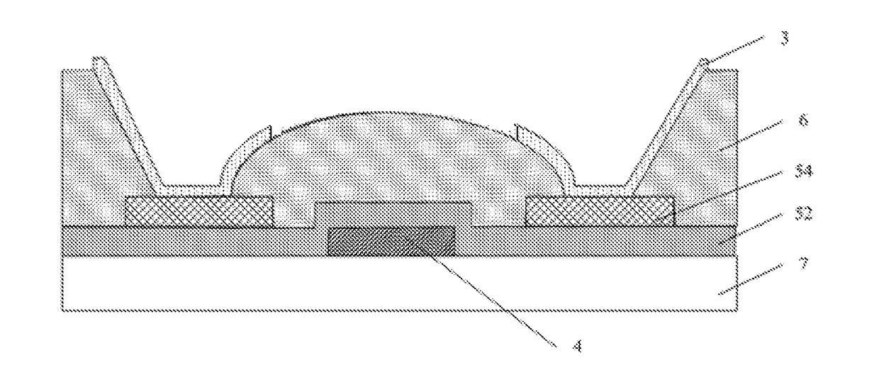
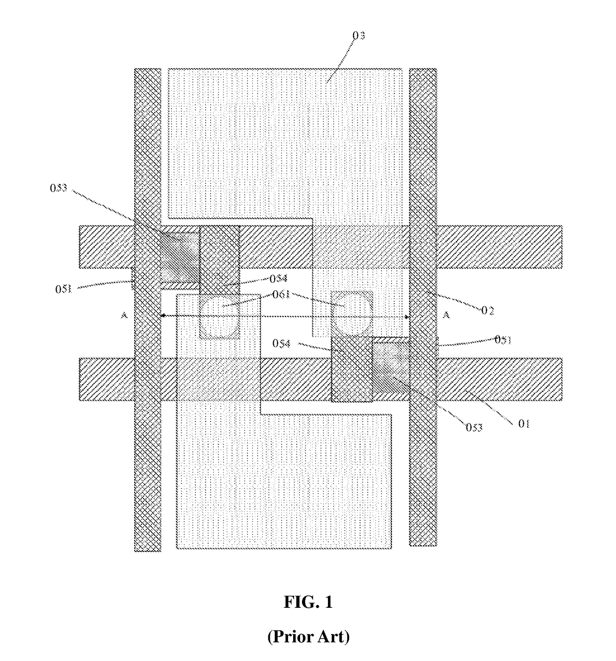
[0051]As shown in FIGS. 4-7, the array substrate includes a display region and a non-display region surrounding the display region. The display region is configured with gate lines 1 and data lines 2. The gate lines 1 and the data lines 2 are crossly configured to define pixel cells. The pixel cell is configured with a thin film transistor. The fir...
second exemplary embodiment
The Second Exemplary Embodiment
[0078]The present embodiment provides an array substrate. The array substrate is suitable for the twisted nematic (TN) mode liquid crystal display device. Compared to the first embodiment, the array substrate includes only the resin layer and the pixel electrode above the thin film transistor, but does not include a common electrode in the array substrate.
[0079]The specific distribution of the pixel structures of the array substrate is illustrated in FIG. 4. The liquid crystal display device includes an array substrate, a counter-configured color filter substrate, and the liquid crystals contained between the two substrates. The pixel electrode 3 is plate shaped. The pixel electrode 3 of the array substrate and a common electrode in the color filter substrate are coordinated to form the electric field to make liquid crystal molecules rotate to display images.
[0080]The array substrate according to the present embodiment includes other structures similar...
third exemplary embodiment
The Third Exemplary Embodiment
[0082]The present embodiment provides an array substrate. Compared to the first and second embodiments, the array substrate has different arrangement of the pixel structures.
[0083]In the present embodiment, a thin film transistor is configured in each pixel cell. The thin film transistor in each pixel cell is configured in a pixel cell defined by the two adjacent rows / columns of data lines. The scenario of shortened distance between the two thin film transistors of the first and second embodiments is not applicable. The light compensating structure is configured under the resin layer surrounding the resin-layer-via-hole corresponding to the drain electrode of the thin film transistor.
[0084]In the present embodiment, the problematic area is defined as the portion of the resin layer surrounding the resin-layer-via-hole corresponding to the drain electrode of the thin film transistor. The problematic area has a thickness thinner than the thickness configur...
PUM
| Property | Measurement | Unit |
|---|---|---|
| thickness | aaaaa | aaaaa |
| thickness | aaaaa | aaaaa |
| insulating | aaaaa | aaaaa |
Abstract
Description
Claims
Application Information
 - R&D
- Intellectual Property
- Life Sciences
- Materials
- Tech Scout
- Unparalleled Data Quality
- Higher Quality Content
- 60% Fewer Hallucinations
Browse by: Latest US Patents, China's latest patents, Technical Efficacy Thesaurus, Application Domain, Technology Topic, Popular Technical Reports.
© 2025 PatSnap. All rights reserved.Legal|Privacy policy|Modern Slavery Act Transparency Statement|Sitemap|About US| Contact US: help@patsnap.com