System and Method for Wafer-Scale Fabrication of Free Standing Mechanical and Photonic Structures By Ion Beam Etching

a technology of ion beam etching and free-standing mechanical and photonic structures, which is applied in the field of nanostructures, can solve the problems of difficult to reproduce consistent device cross sections, poor optical and mechanical properties of films, and inability to readily obtain high-quality thin film heterolayers. to achieve the effect of facilitating undercutting

Active Publication Date: 2018-05-17
PRESIDENT & FELLOWS OF HARVARD COLLEGE
View PDF6 Cites 6 Cited by
  • Summary
  • Abstract
  • Description
  • Claims
  • Application Information

AI Technical Summary

Problems solved by technology

However, for several materials such as diamond, lithium niobate (LiNbO3), silicon carbide (SiC), and gallium nitride (GaN), to name a few, high quality thin film heterolayers are not readily available.
However these films tend to have inferior properties, both optically and mechanically, due to grain boundaries, surface roughness, and inherent film stress.
However such techniques are difficult to reproduce consistent device cross sections and limit the final geometry one can fabricate.
This leads to difficultly in producing identical devices along a sample of several millimeters.
Therefore, due to the physical size of the Faraday cage, it's not feasible to perform this type of etching on a wafer scale.
In both cases there is appreciable ion damage to the device layer, which again significantly limits the performance of the resulting devices.

Method used


Image

  • System and Method for Wafer-Scale Fabrication of Free Standing Mechanical and Photonic Structures By Ion Beam Etching
  • System and Method for Wafer-Scale Fabrication of Free Standing Mechanical and Photonic Structures By Ion Beam Etching
  • System and Method for Wafer-Scale Fabrication of Free Standing Mechanical and Photonic Structures By Ion Beam Etching

Examples


Embodiment Construction

[0019]The following definitions are useful for interpreting terms applied to features of the embodiments disclosed herein, and are meant only to define elements within the disclosure. No limitations on terms used within the claims are intended, or should be derived, thereby. Terms used within the appended claims should only be limited by their customary meaning within the applicable arts.

[0020]As used within this disclosure, “plasma” refers to an electrically conductive gas where the density of ions and electrons are approximately equal.

[0021]As used within this disclosure, an “ion beam source” refers a plasma source having a set of grids (ion optics) that enable extraction of a stream of ions.

[0022]Reference will now be made in detail to embodiments of the present invention, examples of which are illustrated in the accompanying drawings. Wherever possible, the same reference numbers are used in the drawings and the description to refer to the same or like parts.

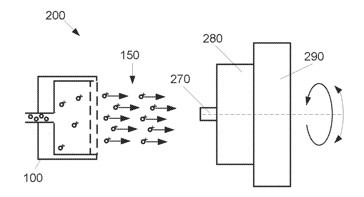
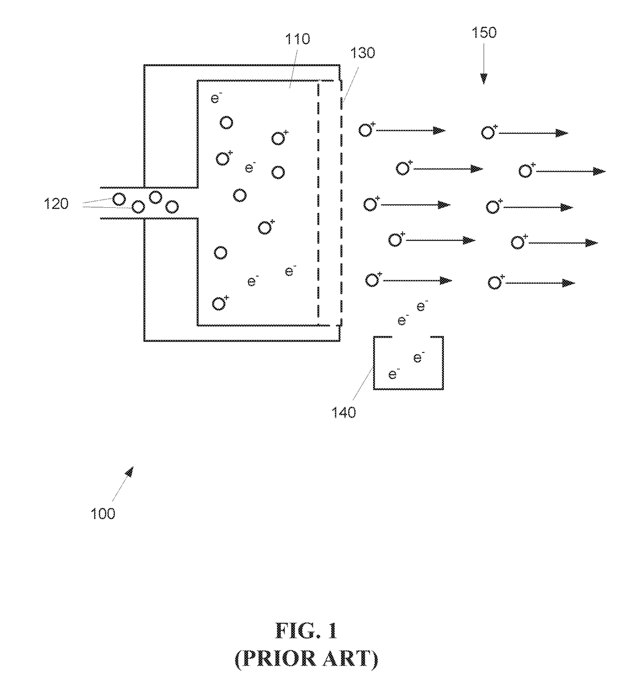
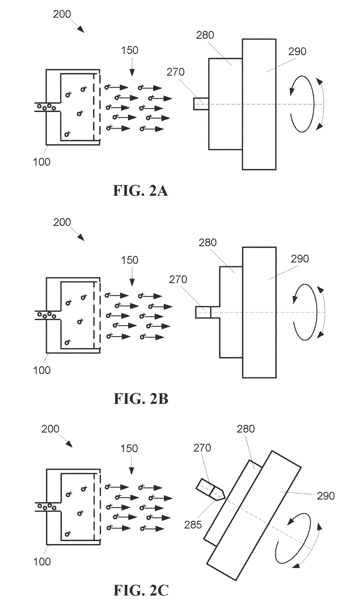
[0023]Exemplary embo...


PUM


Abstract

A method for fabrication of free standing mechanical and photonic structures is presented. A resist mask is applied to a bulk substrate. The bulk substrate is attached to a movable platform. The bulk substrate is exposed to an ion stream produced by a reactive ion beam etching source. The platform is moved relative to the ion stream to facilitate undercutting a portion of the bulk substrate otherwise shielded by the mask.

Description

CROSS-REFERENCE TO RELATED APPLICATIONS[0001]This application claims the benefit of U.S. Provisional Patent Application Ser. No. 62 / 162,058, filed May 15, 2015, entitled “Wafer-scale fabrication of free standing mechanical and photonic structures by ion beam etching,” which is incorporated by reference herein in its entirety.FIELD OF THE INVENTION[0002]The present invention relates to nanostructures, and more particularly, is related to fabrication of free standing mechanical and photonic structures.BACKGROUND OF THE INVENTION[0003]Freestanding nanostructures have many applications in the fields of photonics and mechanics. For photonic devices, refractive index contrast is needed to confine an optical mode. For silicon devices, technologies such as silicon-on-insulator (SOI) can be utilized to achieve refractive index contrast where a high quality silicon device layer is supported by a low index substrate. For nanomechanical resonators and oscillators, mechanical freedom for motion ...

Claims


Application Information

Patent Timeline
Patent Type & Authority Applications(United States)
IPC IPC(8): H01L21/3065B81C99/00
CPCH01L21/3065B81C99/0095B81C2201/0143B81C2201/038B81C2201/056B81B2207/053B81B2207/056
Inventor ATIKIAN, HAIG AVEDISLONCAR, MARKO
Owner PRESIDENT & FELLOWS OF HARVARD COLLEGE
Why Eureka
Try Eureka