
Touch Sensitive Element and Display Device Including the Same

a display device and touch-sensitive technology, applied in the field of touch-sensitive elements and display devices, can solve the problems of easy breakage, inability to provide various vibration feelings of haptic devices, etc., and achieve the effect of small thickness of an electroactive layer

Active Publication Date: 2018-05-03
LG DISPLAY CO LTD
View PDF5 Cites 8 Cited by
  • Summary
  • Abstract
  • Description
  • Claims
  • Application Information

AI Technical Summary

Benefits of technology

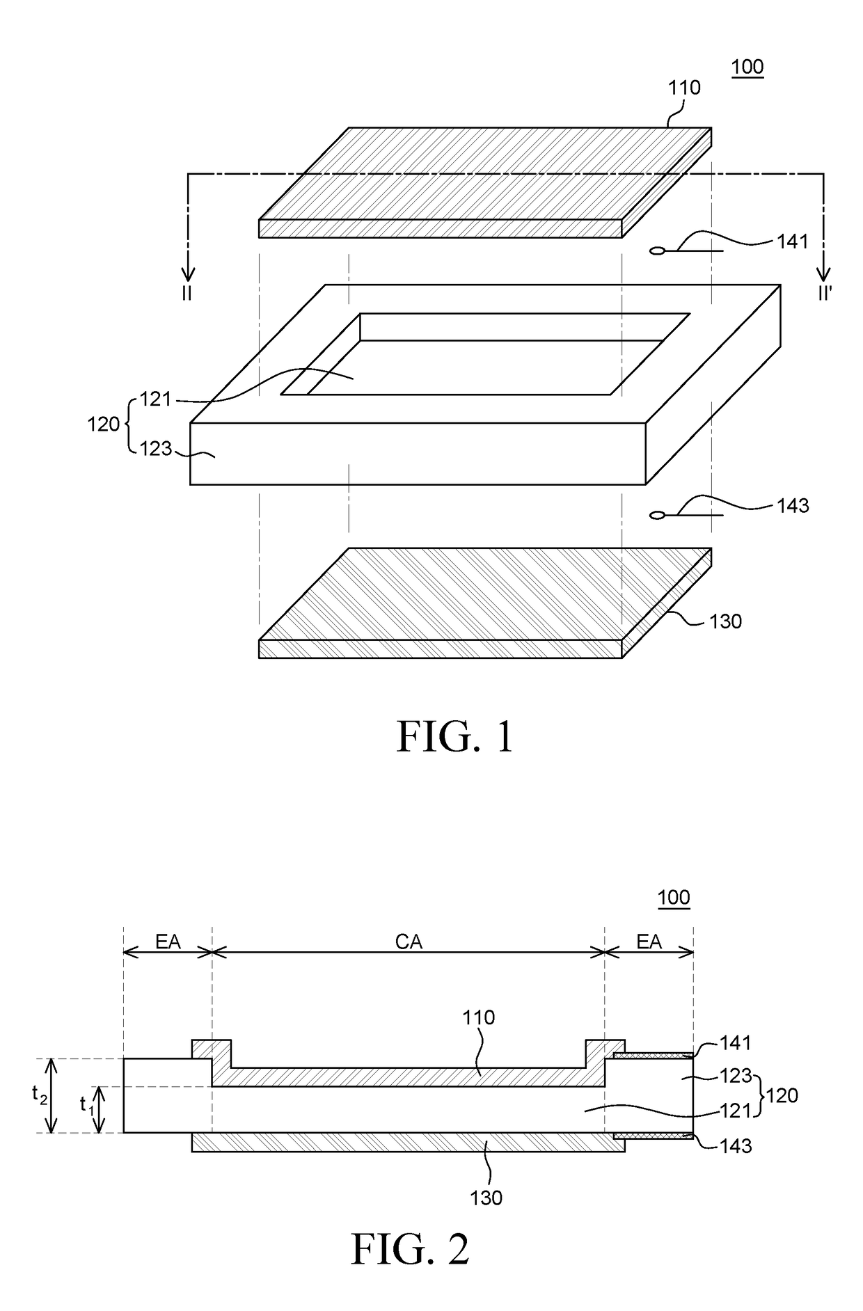
This patent text describes a touch sensitive element that reduces wiring short-circuit defects and improves vibration strength. The element includes an electroactive layer with two different thicknesses: a first portion and a second portion. There are two electrodes that apply a voltage difference to the electroactive layer, which causes it to vibrate. The first portion has a smaller thickness, resulting in an increased intensity of electric field and a higher dielectric breakdown voltage, which reduces the likelihood of short-circuit failures. Additionally, the second portion has a greater thickness, which improves vibration strength. The electroactive layer is designed to have a small thickness in the region where an electrode is placed, which maximizes vibration strength in an upward direction. This touch element is useful in display devices. The technical effects of this design include reduced wiring short-circuit defects, improved vibration strength, and improved tactile feedback for users.

Problems solved by technology

However, the above-mentioned haptic devices are configured by an opaque material and do not vibrate a specific part of the display device, but vibrate the entire display device.
Further, the above-mentioned haptic devices do not provide various vibration feelings and are easily broken by an external impact due to low durability.

Method used


Image

  • Touch Sensitive Element and Display Device Including the Same
  • Touch Sensitive Element and Display Device Including the Same
  • Touch Sensitive Element and Display Device Including the Same

Examples


first exemplary embodiment

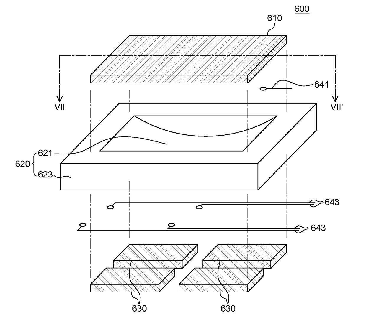
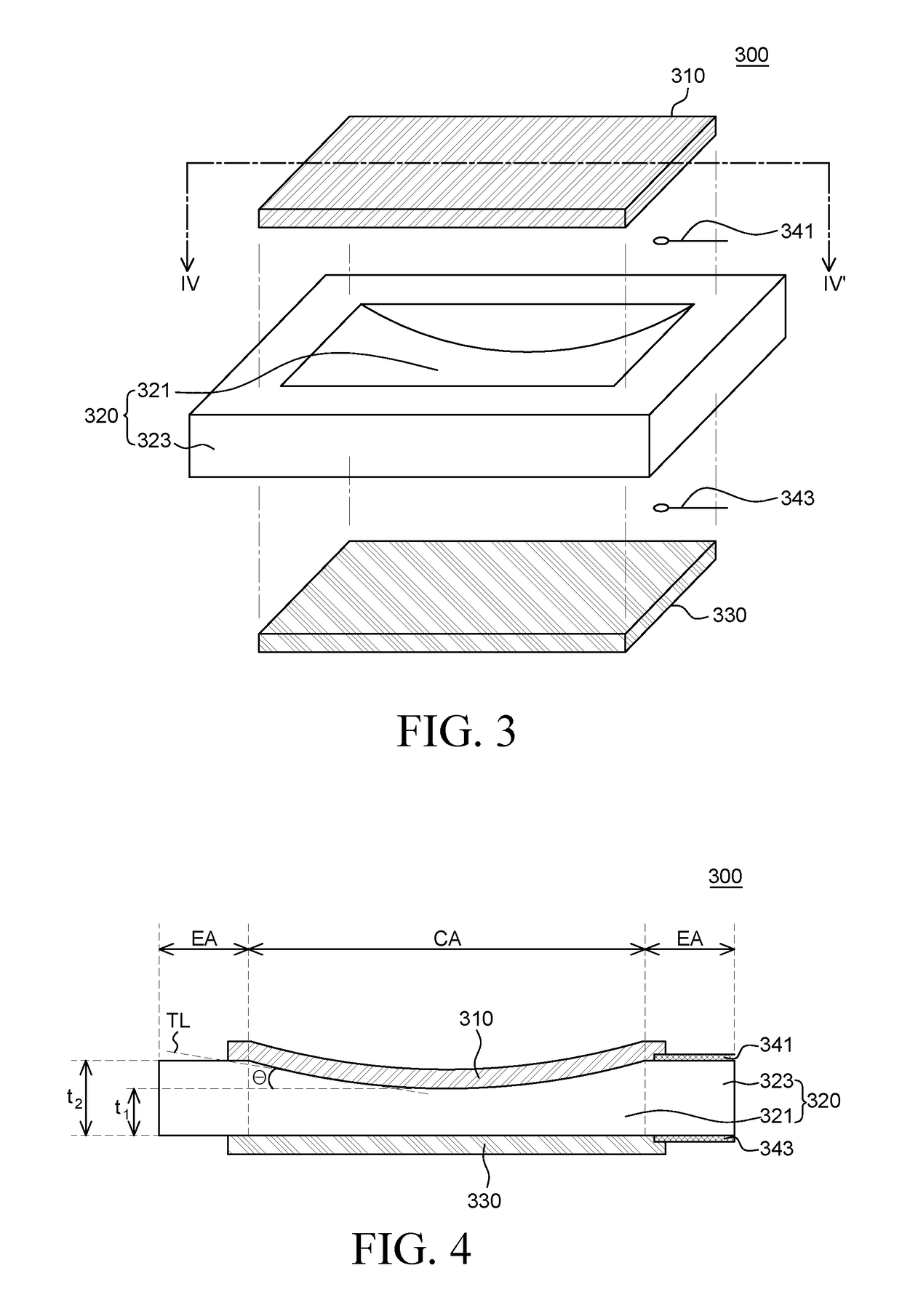
[0087]Specifically, the first thickness of the first portion 321 of the touch sensitive element is 30 μm at a center of the first portion 321 and is gradually increased toward the outside of the first portion 321 from 30 μm to 70 μm. Further, the second thickness of the second portion 323 is 70 μm.

second exemplary embodiment

[0088]In contrast, the first thickness of the first portion 321 of the touch sensitive element is 40 μm at a center of the first portion 321 and is gradually increased toward the outside of the first portion 321 from 40 μm to 70 μm. Further, the second thickness of the second portion 323 is 70 μm.

[0089]A touch sensitive element according to a comparative embodiment is a touch sensitive element to be compared with the touch sensitive element according to the first and second exemplary embodiments. The touch sensitive element according to the comparative embodiment has the same configuration as the touch sensitive element according to the first exemplary embodiment except that it includes an electroactive layer 1020 having the same thickness in all areas. That is, the electroactive layer 1020 of the touch sensitive element according to the comparative embodiment is formed by adding cyano oligomer to PVDF-TrFE-CFE and both a first width w1 and a second width w2 of the electroactive la...


PUM


Abstract

There is provided a touch sensitive element including an electroactive layer, and an electrode disposed on at least one surface of the electroactive layer. The electroactive layer has a first portion having a first thickness and a second portion which has a second thickness different from the first thickness and is in contact with the first portion at an outside of the first portion.

Description

CROSS-REFERENCE TO RELATED APPLICATIONS[0001]This application claims the priority of to Republic of Korean Patent Application No. 10-2016-0143740 filed on Oct. 31, 2016, in the Korean Intellectual Property Office, the disclosure of which is incorporated herein by reference in its entirety.BACKGROUNDField[0002]The present disclosure relates to a touch sensitive element and a display device including the same and more particularly, to a touch sensitive element which reduces a fault rate and generates high vibration with a low driving voltage and a display device including the same.Description of the Related Art[0003]A touch element is a device which senses a user's touch input such as screen touch to a display device and is widely utilized for display devices of public facilities and a large size display device such as a smart television (TV), in addition to a portable display device such as a smart phone or a tablet portable computer (PC). An operation type of the touch element may i...

Claims


Application Information

Patent Timeline
IPC IPC(8): G06F3/01G06F3/041G06F3/044G02F1/1333G02F1/1343
CPCG06F3/016G06F3/0412G06F3/044G02F1/13338G02F1/134363G02F1/133305G06F2203/04112G06F2203/04102H01L27/323G06F3/041H10N30/206H10N30/857G02F1/1336G02F1/133308G02F1/133382H10K59/40H10N30/00H10N30/877H10N30/2048
Inventor LEE, YONGWOOHAM, YONGSUKIM, TAEHEONRYU, KYUNGYEOLKHO, YUSEONLIM, MYUNGJINCHOI, SEULGI
Owner LG DISPLAY CO LTD
Learn More