Nanoscale electronic spin filter
a technology of electronic spin filter and nano-scale, applied in nanoinformatics, magnetic bodies, substrate/intermediate layers, etc., can solve the problems of a few tens of percent magnetoresistance, and the challenge of achieving high spin polarization, so as to achieve a new level of control over spin transport and manipulate spin transport properties effectively.
- Summary
- Abstract
- Description
- Claims
- Application Information
AI Technical Summary
Benefits of technology
Problems solved by technology
Method used
Image


Examples
example 1
Formation of a Junction and Conductance Measurements
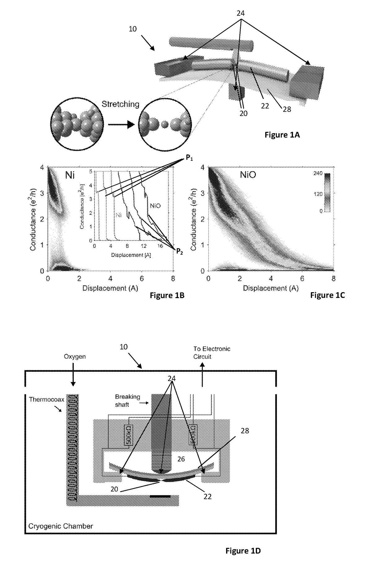
[0138]Reference is made to FIGS. 1A-1D describing experiments carried out by the inventors to investigate electronic spin transport in nickel-oxygen (NiO) junctions. FIGS. 1A and 1D schematically illustrate set ups 10 used for in-situ formation of a nickel-oxygen (NiO) atomic junction within the mechanical break junction setup. FIGS. 1B and 1C show the density plots of conductance vs. inter-electrode displacement for Ni atomic contacts, before (FIG. 1B) and after (FIG. 1C) the introduction of oxygen. In this experiment, the NiO atomic junction was formed in cryogenic conditions (4.2K) using the break-junction setup 10.
[0139]As a first step, Ni atomic contacts 20 were created by breaking a Ni wire 22 using a 3-point bending mechanism, generally designated 24, driven by a piezoelectric element 26 (FIG. 1D). As shown more specifically in FIG. 1D, the mechanically controllable break junction setup 10 is located within a cryogenic chamb...
example 2
Comparison Between Conductance During Junction Pull and Push Back
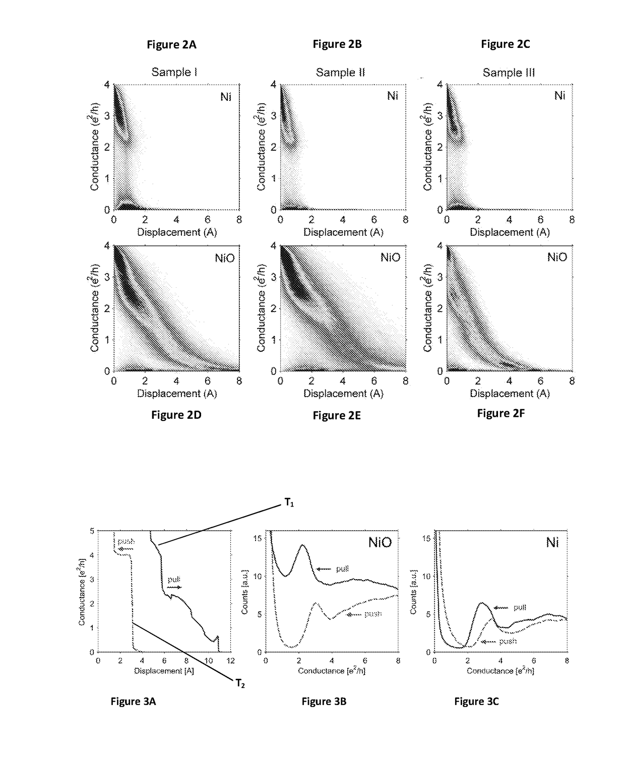
[0152]The clear effect of oxygen on the conduction characteristics of the junction is well observed when the junction is pulled apart. The inventors have found that, when the broken tips are brought back to contact, the transport characteristics do not show a similar indication for the presence of oxygen. FIGS. 3A to 3C exemplify trace recorded on a NiO junction when the junction is elongated and when the broken tips are brought back to contact (FIG. 3A), and conductance histograms for NiO (FIG. 3B) and bare Ni (FIG. 3C). The trace recorded after the insertion of oxygen, as shown in FIG. 3A, has two parts: the pull trace (T1), measured during the elongation of the junction, and the push trace (T2), obtained as the tips are pushed towards each other. Conductance histograms illustrate the distribution of conductance value for 10,000 pull traces and 10,000 push traces for NiO and bare Ni.
[0153]It can be seen that the pull...
example 3
Conductance at Junction Break
[0157]Reference is made to FIGS. 4A-4C, showing pull traces for Ni (curve P1) and NiO (curve P2), where arrows mark the rupture of the contact (FIG. 4A); distribution of the last conductance value measured prior to contact rupture Gbreak for bare Ni and NiO junctions (FIG. 4B); and distribution of the elongations from (4e2) / h until rupture for bare Ni and NiO junctions (FIG. 4C). To obtain the contact rupture Gbreak, the inventors utilized an advantage of the appearance of a discontinuity in the conductance prior to rupture (i.e. FIG. 4A). For each trace, contact rupture Gbreak was set as the conductance value appearing before the last discontinuity with a conductance difference larger than 0.1 e2 / h. Using this approach, a reliable procedure can be defined for the detection of Gbreak that is not confounded by tunneling contributions. FIG. 4B shows a comparison between the distributions of Gbreak calculated for bare Ni (P1) and NiO (P2) junctions. For the...
PUM
| Property | Measurement | Unit |
|---|---|---|
| thickness | aaaaa | aaaaa |
| temperature | aaaaa | aaaaa |
| temperature | aaaaa | aaaaa |
Abstract
Description
Claims
Application Information
 - R&D
- Intellectual Property
- Life Sciences
- Materials
- Tech Scout
- Unparalleled Data Quality
- Higher Quality Content
- 60% Fewer Hallucinations
Browse by: Latest US Patents, China's latest patents, Technical Efficacy Thesaurus, Application Domain, Technology Topic, Popular Technical Reports.
© 2025 PatSnap. All rights reserved.Legal|Privacy policy|Modern Slavery Act Transparency Statement|Sitemap|About US| Contact US: help@patsnap.com