
Vertical Light-Emitting Diode Device and Method of Fabricating the Same

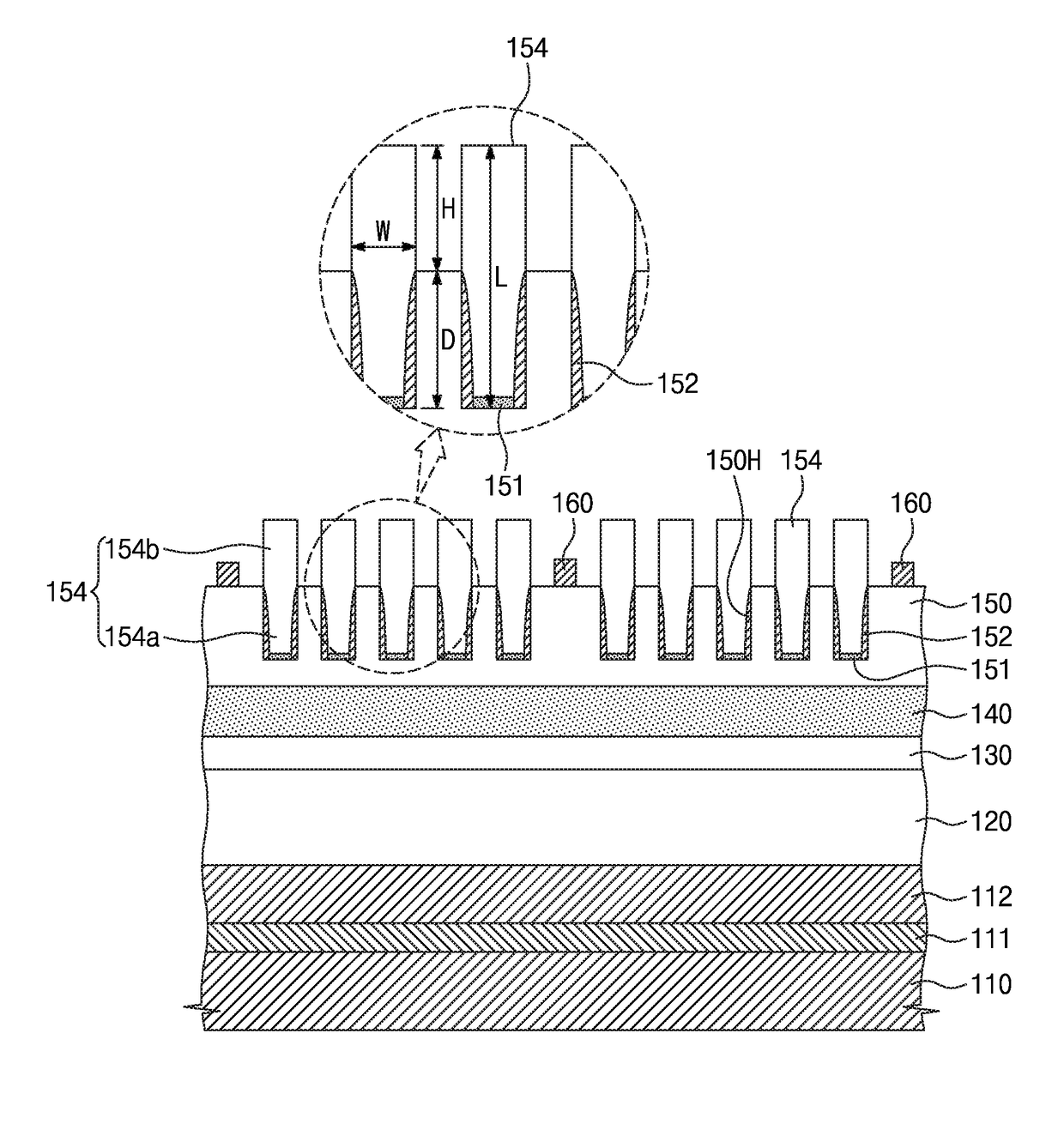
a technology of light-emitting diodes and diodes, which is applied in the direction of semiconductor devices, basic electric elements, electrical equipment, etc., can solve the problem of large fraction of total light reflection, and achieve the effect of increasing the amount of light and suppressing the total reflection

Active Publication Date: 2018-01-04
KOREA UNIV RES & BUSINESS FOUND
View PDF4 Cites 0 Cited by
  • Summary
  • Abstract
  • Description
  • Claims
  • Application Information

AI Technical Summary

Benefits of technology

The invention relates to a vertical light-emitting diode device. Its technical effect is to reduce the reflection of light at the interface between a nitride semiconductor layer and air, resulting in more light emitted from the active layer.

Problems solved by technology

However, due to a large difference in refractive index between the nitride semiconductor layer and the air, a critical angle is very small, and thus, a large fraction of light is totally reflected.

Method used


Image

  • Vertical Light-Emitting Diode Device and Method of Fabricating the Same
  • Vertical Light-Emitting Diode Device and Method of Fabricating the Same
  • Vertical Light-Emitting Diode Device and Method of Fabricating the Same

Examples


Embodiment Construction

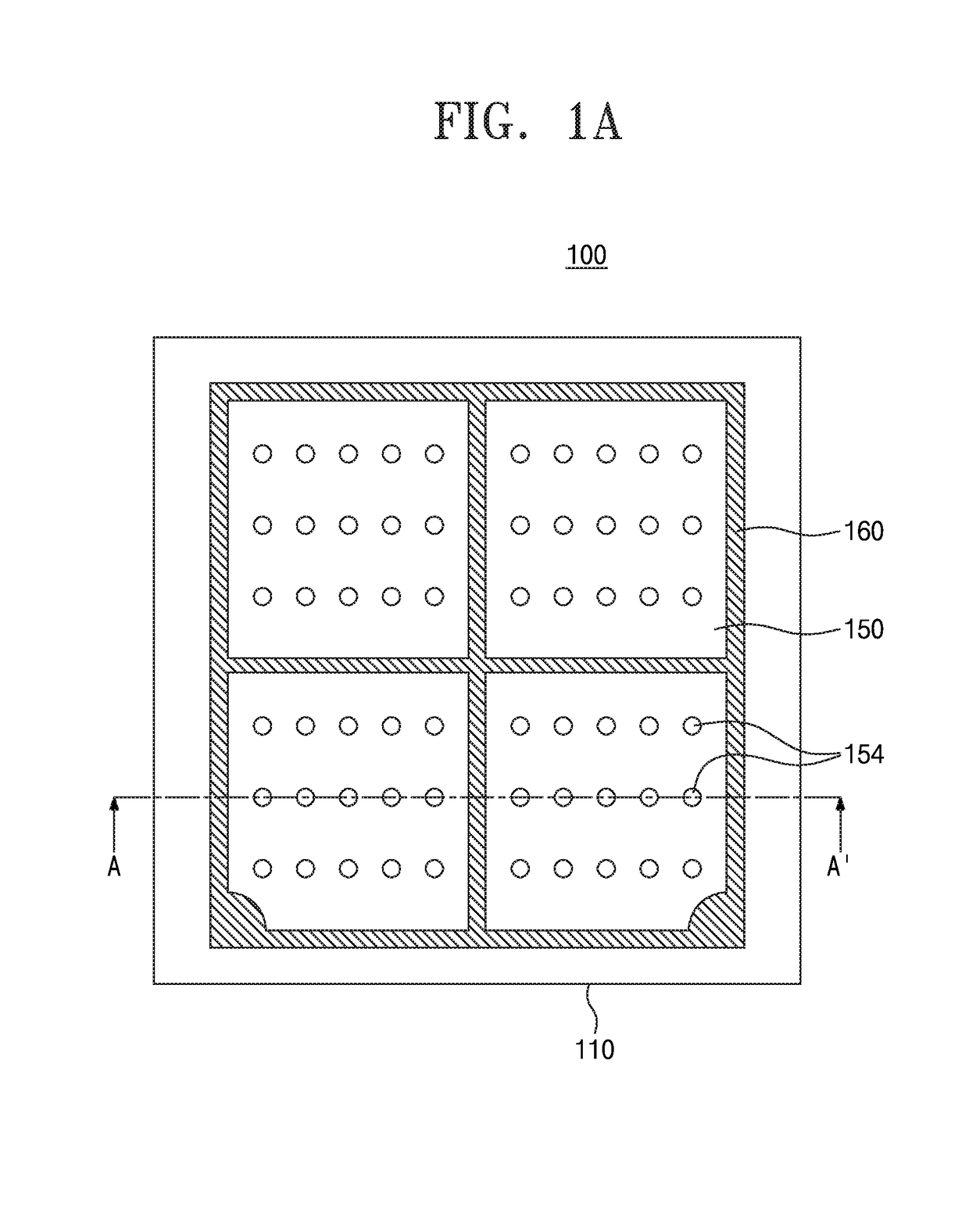
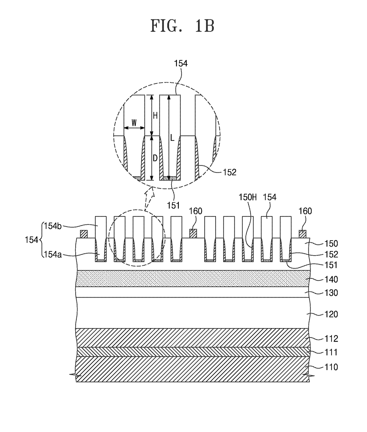
[0030]When light propagates from a dense medium to a sparse medium, the light may be totally reflected by an interface between the two media, and this phenomenon is called ‘total reflection’. The total reflection may occur in a light-emitting diode in which a group III nitride-based material is used. Gallium nitride (GaN) having a refractive index of about 2.4 is a group III nitride-based material which is being generally used for an n-type semiconductor layer, a p-type semiconductor layer, and an active layer. Since there is no substantial difference in refractive index, light generated in the active layer is allowed to propagate toward the n- or p-type semiconductor layer without any difficulty. However, since a difference in refractive index between gallium nitride (GaN) and the air is considerably large, most of the light may be totally reflected by an interface between the n- or p-type semiconductor layer and the air. According to some embodiments of the inventive concept, ligh...


PUM


Abstract

A vertical light-emitting diode device and a method of fabricating the same are provided. The device may include a conductive substrate serving as a p electrode, a p-type GaN layer provided on the conductive substrate, an active layer provided on the p-type GaN layer, an n-type GaN layer provided on the active layer, an n electrode pattern provided on the n-type GaN layer, a metal oxide structure filling a plurality of holes formed in the n-type GaN layer, and a seed layer provided on bottom surfaces of the holes and used to as a seed in a crystal growth process of the metal oxide structure.

Description

CROSS-REFERENCE TO RELATED APPLICATIONS[0001]This U.S. non-provisional patent application claims priority under 35 U.S.C. §119 to Korean Patent Application No. 10-2016-0083693, filed on Jul. 1, 2016, in the Korean Intellectual Property Office, the entire contents of which are hereby incorporated by reference.BACKGROUND OF THE INVENTION[0002]The present disclosure relates to a vertical light-emitting diode device and a method of fabricating the same. The formation of the vertical light-emitting diode device may include forming holes in an n-type GaN layer, forming a sidewall, which is made of a metal, metal alloy, or dielectric material, on an inner side surface of each of the holes, and growing a metal oxide structure from a bottom surface of each of the holes.[0003]Thus, when light is totally reflected inward from an interface between the n-type GaN layer and the air, the light may be emitted through the metal oxide structure. This may make it possible to realize a vertical light-e...

Claims


Application Information

Patent Timeline
Patent Type & Authority Applications(United States)
IPC IPC(8): H01L33/24H01L33/32H01L33/00
CPCH01L33/24H01L33/0075H01L33/32H01L33/20H01L33/38H01L33/00H01L33/0008H01L33/005H01L33/0093H01L33/02H01L33/36H01L2924/12041H01L33/30H01L33/40H01L33/42
Inventor SEONG, TAE YEONKIM, KI SEOKSONG, SUNG-JOO
Owner KOREA UNIV RES & BUSINESS FOUND
Learn More