
Pattern processing method, method for manufacturing semiconductor substrate product, and pretreatment liquid for pattern structure

Inactive Publication Date: 2017-12-21
FUJIFILM CORP
View PDF12 Cites 2 Cited by
  • Summary
  • Abstract
  • Description
  • Claims
  • Application Information

AI Technical Summary

Benefits of technology

The present invention provides a method and a pretreatment liquid for pattern processing that are suitable for polysilicon, amorphous silicon, germanium, or low dielectric constant materials with a low k value. The pretreatment liquid can prevent pattern collapse and suppress damage caused by chemicals. This invention effectively prevents damage to the pattern structure and improves reliability during semiconductor device manufacturing.

Problems solved by technology

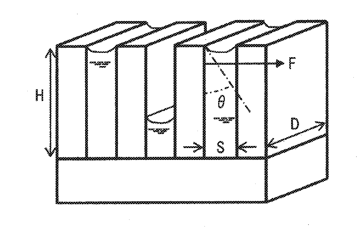
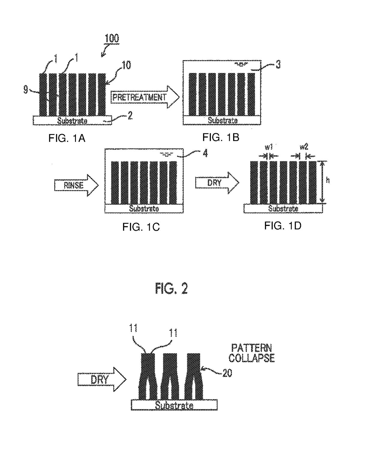
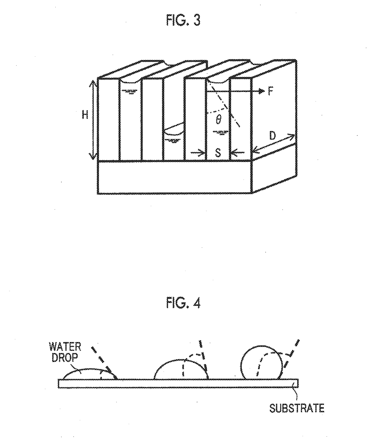
Particularly, there is a problem in the collapse of pattern of the structure occurring due to an increase in the aspect ratio thereof.
The treatment liquid or the cleaning liquid is evaporated at the time of drying, but the pattern is affected by surface tension during the process and is thus drawn to cause a collapse.
It is required to design a pattern structure which does not cause such a pattern collapse, and the degree of freedom in designing is limited with the fine pattern formation.

Method used


Image

  • Pattern processing method, method for manufacturing semiconductor substrate product, and pretreatment liquid for pattern structure
  • Pattern processing method, method for manufacturing semiconductor substrate product, and pretreatment liquid for pattern structure
  • Pattern processing method, method for manufacturing semiconductor substrate product, and pretreatment liquid for pattern structure

Examples


example 1

[0174]A wafer in which films of each material shown in Table (solid films, that is, clean single films for an evaluation shown in the following to ) was prepared. A treatment was carried out with 5% HF to remove the natural oxide film. The wafer after the pretreatment was used to conduct a beaker test. Specifically, while stirring the chemical liquid at room temperature at 250 rpm, the wafer was put into a beaker to carry out the pretreatment with each pretreatment liquid for 5 minutes. The wafer after the treatment was rinsed with flowing water (ultrapure water) for 5 seconds and dried with N2 gas. The temperature at the time of drying was set to 20° C. (room temperature).

[0175]The contact angle of the wafer which had been subjected to a treatment with the pretreatment liquid was measured with the following contact angle device using water. This is an alternative measure of the above-described θCA and as this value increases, θCA decreases. As a result, it can be said that the cap...


PUM


Abstract

Provided are a pattern processing method for applying a pretreatment liquid for modifying the surface of a pattern structure to a semiconductor substrate provided with the pattern structure, which has at least one of polysilicon, amorphous silicon, Ge, or a low dielectric constant material having a k value of 2.4 or less, a method for manufacturing a semiconductor substrate product, and a pretreatment liquid for a pattern structure.

Description

CROSS-REFERENCE TO RELATED APPLICATIONS[0001]This application is a Continuation of PCT International Application No. PCT / JP2016 / 051736 filed on Jan. 21, 2016, which claims priority under 35 U.S.C. §119 (a) to Japanese Patent Application No. 2015-011646 filed on Jan. 23, 2015. Each of the above applications is hereby expressly incorporated by reference, in its entirety, into the present application.BACKGROUND OF THE INVENTION1. Field of the Invention[0002]The present invention relates to a pattern processing method, a method for manufacturing a semiconductor substrate product, and a pretreatment liquid for a pattern structure.2. Description of the Related Art[0003]In the manufacturing field through a fine pattern structure of a metal compound such as a semiconductor substrate or a micromachine, a technology for suppressing the collapse of the pattern structure thereof has been demanded. As miniaturization and high integration or an increase in speed of the semiconductor substrate pro...

Claims


Application Information

Patent Timeline
IPC IPC(8): H01L21/306
CPCH01L21/30604H01L21/02057
Inventor PARK, KEEYOUNGMIZUTANI, ATSUSHI
Owner FUJIFILM CORP
Learn More