
Ltps pixel unit and manufacturing method for the same

a technology of pixel units and manufacturing methods, applied in the field of display technology, can solve the problems of difficult to guarantee uniformity of production, large production costs, complicated manufacturing, etc., and achieve the effects of saving manufacturing processes, improving product yield, and saving costs

Inactive Publication Date: 2017-10-19
SHENZHEN CHINA STAR OPTOELECTRONICS TECH CO LTD
View PDF6 Cites 4 Cited by
  • Summary
  • Abstract
  • Description
  • Claims
  • Application Information

AI Technical Summary

Benefits of technology

The present invention provides a method for manufacturing a LTPS pixel unit that saves manufacturing process costs and improves product yield. By forming a semiconductor pattern and a common electrode pattern with an interval on a buffering layer, we can sequentially form layers of insulation and electrodes without needing a thicker organic layer. This allows for better electrical contact and reduces the risk of defects in the final product. Overall, the invention provides a more efficient and cost-effective method for producing LTPS pixel units.

Problems solved by technology

A conventional pixel unit of the LTPS display has many layers and structures, and is very complicated to manufacture.
As a result, the production cost is large.
Accordingly, the organic layer pattern is required to be thick such that the uniformity of the production is hard to guarantee.

Method used


Image

  • Ltps pixel unit and manufacturing method for the same
  • Ltps pixel unit and manufacturing method for the same
  • Ltps pixel unit and manufacturing method for the same

Examples


Embodiment Construction

[0023]The following will combine drawings and embodiments for detailed description of the present invention.

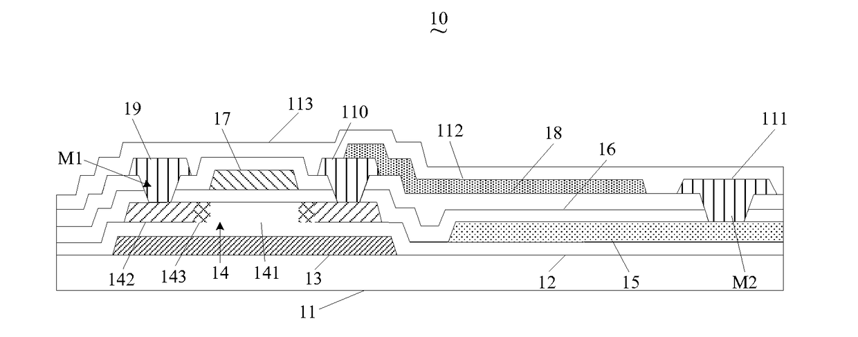
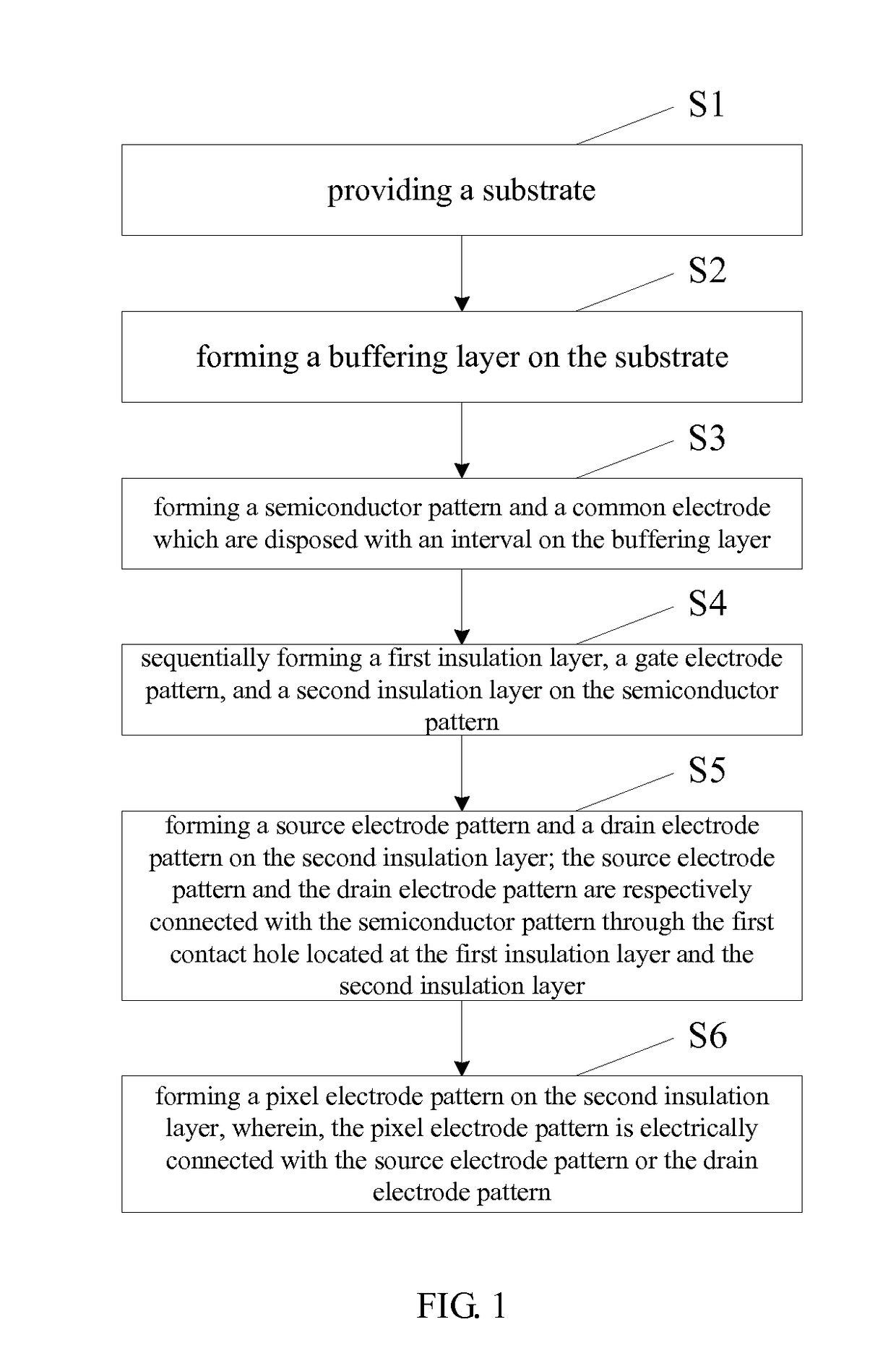
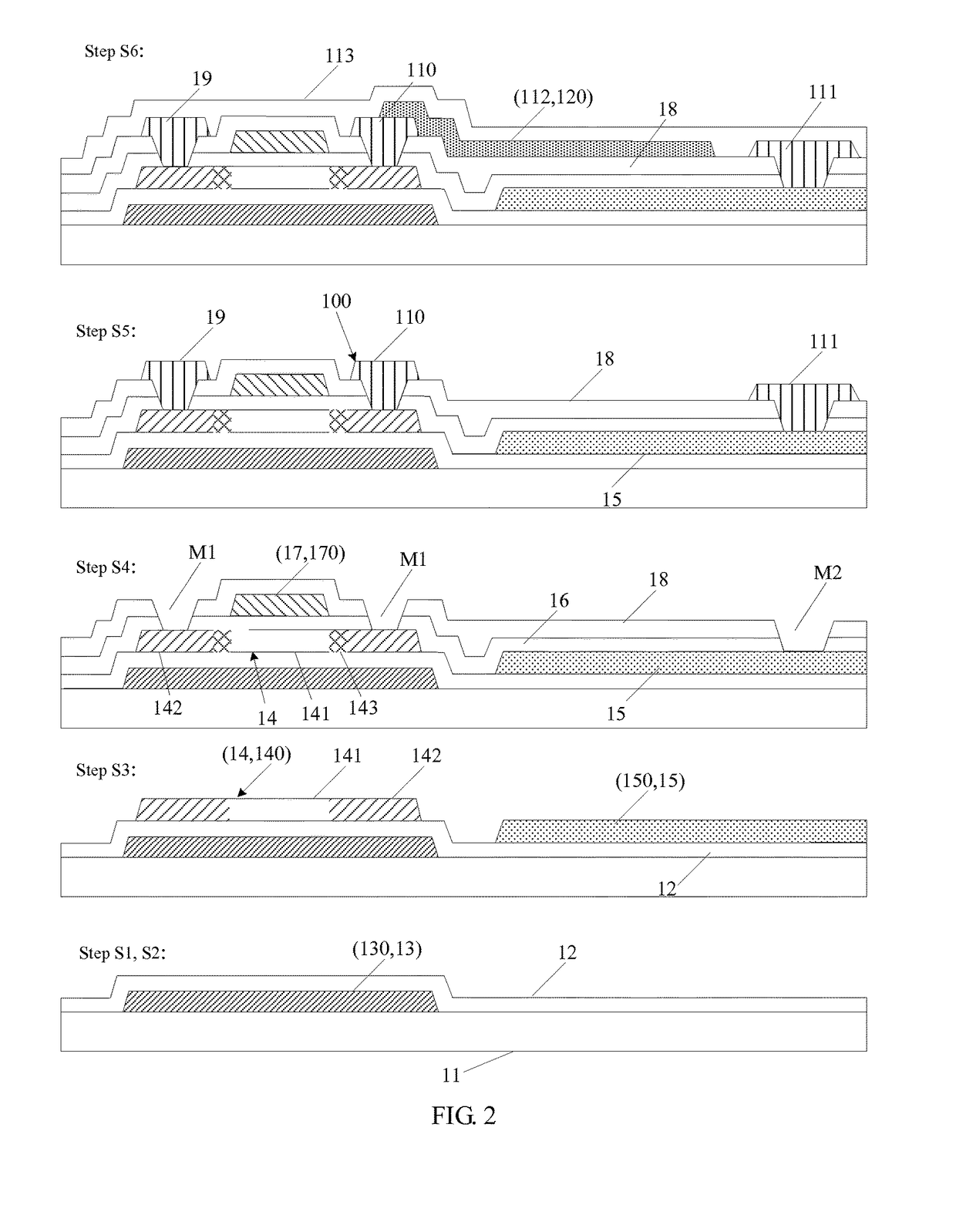
[0024]With reference to FIG. 1, FIG. 1 is a flowchart of a manufacturing method for an LTPS pixel unit according to an embodiment of the present invention. The manufacturing method of the LTPS pixel unit of the present invention including following steps:

[0025]Step S1: providing a substrate 11.

[0026]Wherein, the substrate 11 is preferably a glass substrate. When providing the substrate 11, cleaning, sanding and other operations to remove impurities on the surface of the substrate 11 at the same time. Then, through a drying step to dry the substrate 11 so as to provide a clean substrate 11.

[0027]Step S2: forming a buffering layer 12 on the substrate 11.

[0028]Before step S2, forming a light shielding pattern 13 on the substrate 11. The light shielding pattern 13 is specifically made of a metal material or an amorphous silicon material.

[0029]The specific manufacturing process of ...


PUM


Abstract

An LTPS pixel unit and a manufacturing method. The method includes following steps: forming a buffering layer on the substrate; forming a semiconductor pattern and a common electrode pattern which are disposed with an interval on the buffering layer; sequentially forming a first insulation layer, a gate electrode pattern and a second insulation layer on the semiconductor pattern; forming a source electrode pattern and a drain electrode pattern on the second insulation layer, wherein, the source electrode pattern and the drain electrode pattern electrically contact with the semiconductor pattern through a first contact hole at the first insulation layer and the second insulation layer; and forming a pixel electrode pattern on the second insulation layer, wherein, the pixel electrode pattern electrically contacts with the source electrode pattern or the drain electrode pattern. Accordingly, the present invention can save the cost and increase process yield.

Description

BACKGROUND OF THE INVENTION1. Field of the Invention[0001]The present invention relates to a display technology field, and more particularly to an LTPS pixel unit and a manufacturing method for the same.2. Description of Related Art[0002]In a small size and high-resolution display, an LTPS (Low Temperature Poly-Silicon) display has been widely used due to the high mobility, stable performance characteristics.[0003]A conventional pixel unit of the LTPS display has many layers and structures, and is very complicated to manufacture. Using conventional NMOS manufacturing process as an example, 10 mask processes are required. The specific elements using the mask processes are respectively: a light shielding pattern, a semiconductor pattern, a doped semiconductor pattern, a gate electrode pattern, a first conductive hole for a first and a second insulation layers, a source electrode pattern and a drain electrode pattern, an organic layer pattern, a capacitor electrode pattern, a passivati...

Claims


Application Information

Patent Timeline
Patent Type & Authority Applications(United States)
IPC IPC(8): H01L27/12H01L29/786
CPCH01L27/1288H01L27/127H01L27/1222H01L29/78633H01L29/78675H01L29/78621H01L27/124H10K2102/302H10K71/00H10K59/80H10K71/621H01L29/66757H10K50/80
Inventor HU, YUTONGDU, PENG
Owner SHENZHEN CHINA STAR OPTOELECTRONICS TECH CO LTD
Learn More