Eureka AIR delivers breakthrough ideas for toughest innovation challenges, trusted by R&D personnel around the world.

Pattern forming method as well as production methods for processed substrate, optical component, circuit board, electronic component and imprint mold

a technology of substrate and forming method, which is applied in the direction of instruments, photomechanical devices, other domestic objects, etc., can solve the problems of low throughput and achieve the effect of shortening the filling time of sst-nil and high throughpu

Active Publication Date: 2017-10-05
CANON KK
View PDF5 Cites 20 Cited by
  • Summary
  • Abstract
  • Description
  • Claims
  • Application Information

AI Technical Summary

Benefits of technology

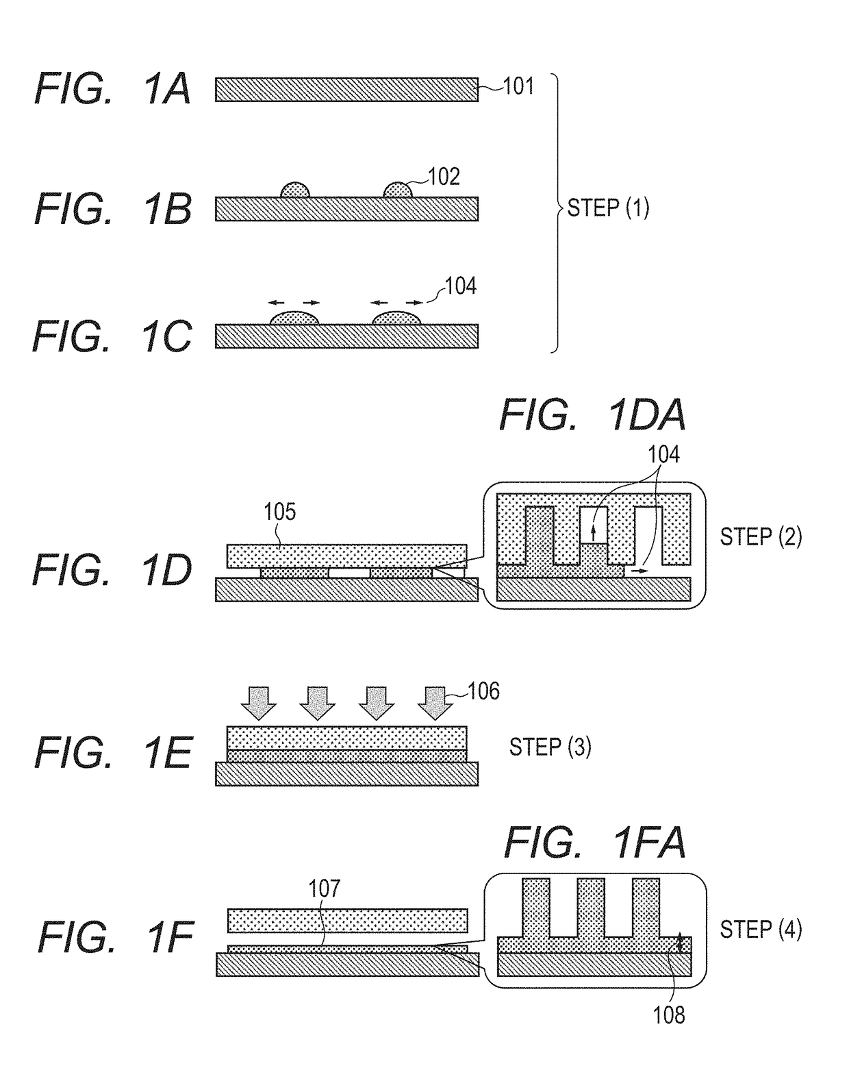
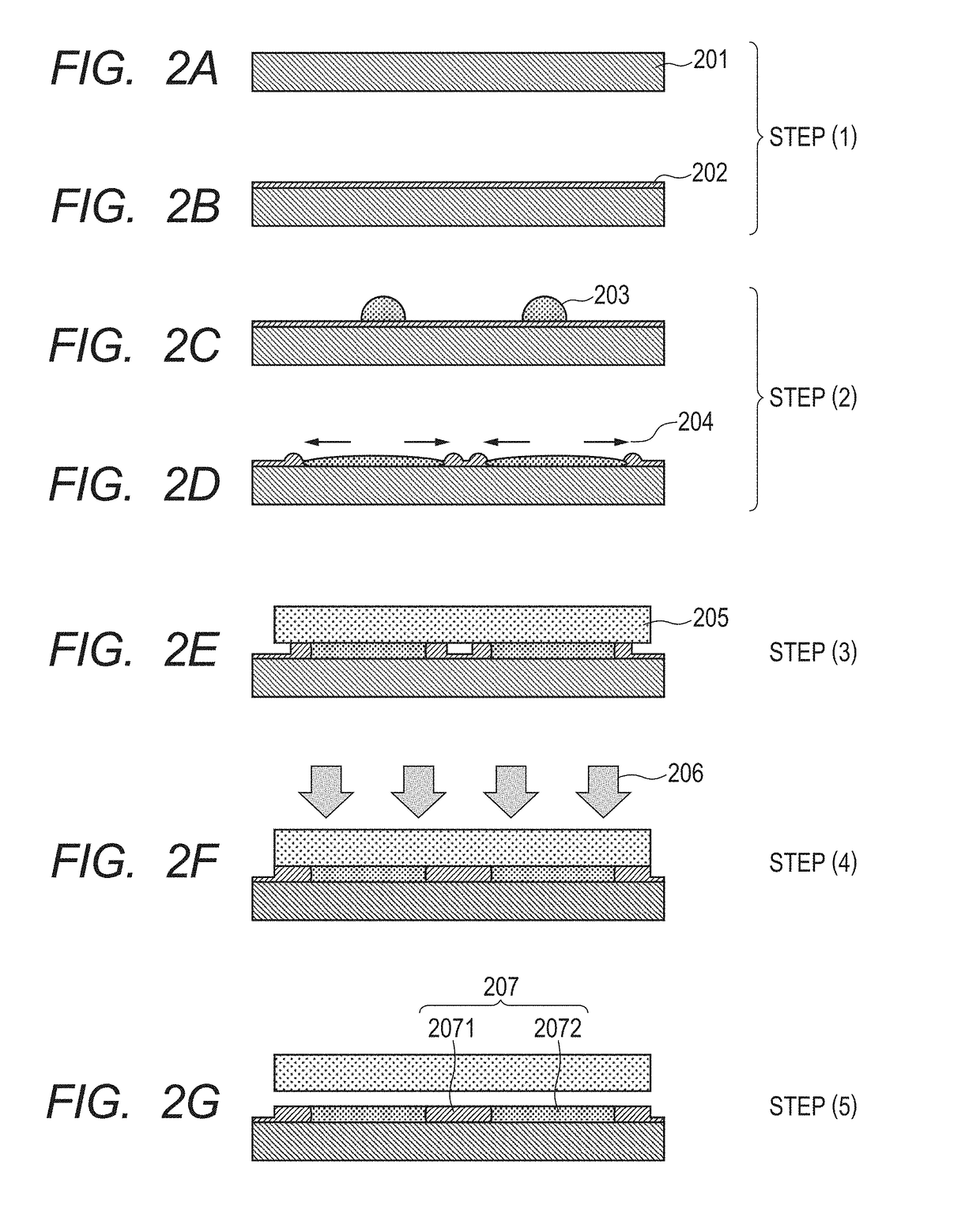
The present invention provides a method for forming patterns using a curable composition in a high-throughput manner while minimizing release defects. The invention utilizes the Marangoni effect, which results in a faster prespread of a low surface tension liquid over a wider surface area when dispensed over a high surface tension liquid. This allows for faster filling of the mold and reduces the time required for the pattern formation process. Additionally, the invention incorporates a fluorine-based release agent that helps prevent release defects when incorporated into the curable composition. Overall, this method results in higher throughput and fewer release defects.

Problems solved by technology

The photo-nanoimprint technology disclosed in Japanese Patent No. 4791357 has involved a problem in that a time period (filling time) from the initiation of the contact of the mold to the completion of the spread and the fill is long, and hence throughput is low.

Method used


Image

  • Pattern forming method as well as production methods for processed substrate, optical component, circuit board, electronic component and imprint mold
  • Pattern forming method as well as production methods for processed substrate, optical component, circuit board, electronic component and imprint mold
  • Pattern forming method as well as production methods for processed substrate, optical component, circuit board, electronic component and imprint mold

Examples


example 1

[0182](1) Preparation of Curable Composition (A1-1)

[0183]A component (a1), a component (b1), a component (c1), and a component (d1) described below were blended, and the blend was filtered with a 0.2-micrometer filter made of ultrahigh-molecular weight polyethylene to prepare a curable composition (A1-1) of Example 1.

[0184](1-1) Component (a1):[0185]94 parts by weight in total

[0186]Isobornyl acrylate (manufactured by Kyoeisha Chemical Co., Ltd., trade name: IB-XA):[0187]9 parts by weight

[0188]Benzyl acrylate (manufactured by Osaka Organic Chemical Industry Ltd., trade name: V*160):[0189]38 parts by weight

[0190]Neopentyl glycol diacrylate (manufactured by Kyoeisha Chemical Co., Ltd., trade name: NP-A):[0191]47 parts by weight

[0192](1-2) Component (b1):[0193]0 parts by weight in total

[0194]The component (b1) was not added.

[0195](1-3) Component (c1):[0196]1.1 parts by weight in total

[0197]Polyoxyethylene stearyl ether (EO 5 mol aduct) (manufactured by Aoki Oil Industrial Co., Ltd., tra...

example 2

[0236](1) Curable Composition (A1-2)

[0237]A component (a1), a component (b1), a component (c1), and a component (d1) described below were blended, and the blend was filtered with a 0.2-micrometer filter made of ultrahigh-molecular weight polyethylene to prepare a curable composition (A1-2) of Example 2.

[0238](1-1) Component (a1):[0239]94 parts by weight in total

[0240]The same formulation as that of Example 1 was adopted.

[0241](1-2) Component (b1):[0242]0 parts by weight in total

[0243]The component (b1) was not added in the same manner as in Example 1.

[0244](1-3) Component (c1):[0245]1.1 parts by weight in total

[0246]Polyoxyethylene stearyl ether (EO 15 mol aduct) (manufactured by Aoki Oil Industrial Co., Ltd., trade name: BLAUNON SR-715):[0247]1.1 parts by weight

[0248](1-4) Component (d1):[0249]33,000 parts by weight in total

[0250]The same component as that of Example 1 was adopted.

[0251](2) Measurement of Surface Tension of Curable Composition (A1-2)

[0252]The surface tension of a c...

example 3

[0262](1) Curable Composition (A1-3)

[0263]A component (a1), a component (b1), a component (c1), and a component (d1) described below were blended, and the blend was filtered with a 0.2-micrometer filter made of ultrahigh-molecular weight polyethylene to prepare a curable composition (A1-3) of Example 3.

[0264](1-1) Component (a1):[0265]94 parts by weight in total

[0266]The same formulation as that of Example 1 was adopted.

[0267](1-2) Component (b1):[0268]0 parts by weight in total

[0269]The component (b1) was not added in the same manner as in Example 1.

[0270](1-3) Component (c1):[0271]1.1 parts by weight in total

[0272]Polyoxyethylene stearyl ether (EO 30 mol aduct) (manufactured by Aoki Oil Industrial Co., Ltd., trade name: BLAUNON SR-730):[0273]1.1 parts by weight

[0274](1-4) Component (d1):[0275]33,000 parts by weight in total

[0276]The same component as that of Example 1 was adopted.

[0277](2) Measurement of Surface Tension of Curable Composition (A1-3)

[0278]The surface tension of a c...


PUM

PropertyMeasurementUnit
Temperatureaaaaaaaaaa
Fractionaaaaaaaaaa
Volumeaaaaaaaaaa

Abstract

A pattern is formed on a substrate with forming a layer of a curable composition (A1) containing a component (a1) as a polymerizable compound and a component (c1) as a surfactant on a surface of the substrate, then dispensing droplets of a curable composition (A2) containing a component (a2) as a polymerizable compound and a component (c2) as a surfactant dropwise discretely onto the layer formed of the curable composition (A1), subsequently sandwiching a mixture layer of the curable composition (A1) and the curable composition (A2) between a mold having a pattern and the substrate, then irradiating the mixture layer with light to cure the mixture layer, and releasing the mold from the mixture layer after the curing. The curable composition (A1) containing at least 0.5 wt % or more of the component (c1), the curable composition (A2) containing at least 0.5 wt % or more of the component (c2).

Description

BACKGROUND OF THE INVENTIONField of the Invention[0001]The present invention relates to a pattern forming method, a method of producing a processed substrate, a method of producing an optical component, a method of producing a circuit board, a method of producing an electronic component, and a method of producing an imprint mold.Description of the Related Art[0002]There has been a growing requirement for miniaturization in a semiconductor device, a MEMS, or the like, and hence a photo-nanoimprint technology has been attracting attention as a microfabrication technology.[0003]In the photo-nanoimprint technology, a photocurable composition (resist) is cured in a state in which a mold having a fine groove / land pattern formed on its surface is pressed against a substrate (wafer) having applied thereto the photocurable composition. Thus, the groove / land pattern of the mold is transferred onto the cured film of the photocurable composition and hence the pattern is formed on the substrate....

Claims


Application Information

Patent Timeline
IPC IPC(8): G03F7/00C09D4/00
CPCC09D4/00G03F7/0002C08F222/10C08F220/1811B05D1/30B05D3/04B05D3/12B29C59/026G03F7/161B29L2011/00B29L2031/34
Inventor CHIBA, KEIKOITO, TOSHIKILIU, WEIJUNSTACHOWIAK, TIMOTHY BRIANKHUSNATDINOV, NIYAZ
Owner CANON KK
Why Eureka
Eureka Blog
Learn More