
Display device and optical compensation method of a display device

a display device and optical compensation technology, applied in the field of display devices, can solve the problems of inability or inability of the optical compensation method to adequately compensate the grayscale, uneven characteristics of thin film transistors, uneven current-voltage characteristics, etc., to achieve the effect of improving the optical compensation process, and improving the quality of display images

Active Publication Date: 2017-07-20
SAMSUNG DISPLAY CO LTD
View PDF4 Cites 20 Cited by
  • Summary
  • Abstract
  • Description
  • Claims
  • Application Information

AI Technical Summary

Benefits of technology

This patent describes a method to control the timing of light emissions from pixels in a display device. This allows for more precise control over the display and can help reduce issues like staining. The method also provides a simplified way to compensate for variations in brightness across the display. Overall, this method can improve the quality of the displayed image and enhance the overall performance of the display device.

Problems solved by technology

However, thin film transistors may have uneven characteristics (e.g., uneven current-voltage characteristics) due to the crystallization process.
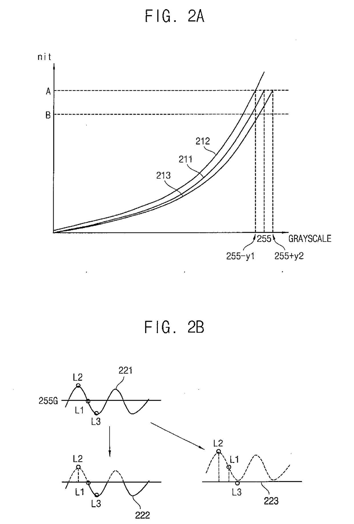
The optical compensation method can compensate a grayscale value when the pixel emits light having a relatively high luminance; however, the optical compensation method cannot or cannot adequately compensate a grayscale value when the pixel emits light having a relatively low luminance because the optical compensation method cannot increase the grayscale value over a maximum grayscale value.

Method used


Image

  • Display device and optical compensation method of a display device
  • Display device and optical compensation method of a display device
  • Display device and optical compensation method of a display device

Examples


Embodiment Construction

[0044]Hereinafter, aspects of the present inventive concept will be explained in detail with reference to the accompanying drawings.

[0045]It will be understood that when an element or layer is referred to as being “on,”“connected to,” or “coupled to” another element or layer, it may be directly on, connected, or coupled to the other element or layer or one or more intervening elements or layers may also be present. When an element is referred to as being “directly on,”“directly connected to,” or “directly coupled to” another element or layer, there are no intervening elements or layers present. For example, when a first element is described as being “coupled” or “connected” to a second element, the first element may be directly coupled or connected to the second element or the first element may be indirectly coupled or connected to the second element via one or more intervening elements. The same reference numerals designate the same elements. As used herein, the term “and / or” inclu...


PUM


Abstract

An optical compensation method for a display device including a pixel is provided. The method includes: providing test data having a first grayscale value to the display device; measuring a luminance of the pixel which emits light based on the test data; and calculating a compensation grayscale value based on a second target luminance and the measured luminance of the pixel. The second target luminance is lower than a first target luminance which is set based on the first grayscale value.

Description

CROSS-REFERENCE TO RELATED APPLICATION[0001]This application claims priority under 35 U.S.C. §119 to and the benefit of Korean Patent Application No. 10-2016-0006311, filed on Jan. 19, 2016 in the Korean Intellectual Property Office (KIPO), the contents of which are incorporated herein in their entirety by reference.BACKGROUND[0002]1. Field[0003]Example embodiments relate to a display device.[0004]2. Description of the Related Art[0005]An organic light emitting display device includes pixels, and each of the pixels includes an organic light emitting diode and a thin film transistor which drives the organic light emitting diode. The thin film transistor may be formed through a crystallization process (e.g., a melting process and a solidification process) of a low-temperature poly-silicon (LTPS). However, thin film transistors may have uneven characteristics (e.g., uneven current-voltage characteristics) due to the crystallization process.[0006]An optical compensation method is propos...

Claims


Application Information

Patent Timeline
IPC IPC(8): G09G3/20
CPCG09G3/2092G09G2320/0646G09G2310/08G09G3/3225G09G2320/0626G09G3/3208G09G2320/0233G09G2320/0276G09G2320/029G09G2320/0673G09G2320/0693
Inventor CHA, UI-YEONGKIM, DAN-BIKIM, IN-HWANJUN, BYUNG-GEUN
Owner SAMSUNG DISPLAY CO LTD
Learn More