
Integrated structures of acoustic wave device and varactor, and acoustic wave device, varactor and power amplifier, and fabrication methods thereof

a technology of integrated structures and acoustic waves, applied in the direction of amplifiers with semiconductor devices/discharge tubes, solid-state devices, basic electric elements, etc., can solve the problems of high materials cost, high equipment cost, time-consuming, etc., and achieve the effect of widening the gap, reducing component size, and optimizing impedance matching

Active Publication Date: 2017-06-15
WIN SEMICON
View PDF3 Cites 8 Cited by
  • Summary
  • Abstract
  • Description
  • Claims
  • Application Information

AI Technical Summary

Benefits of technology

The present invention provides an integrated structure of an acoustic wave device and a varactor on the same semiconductor substrate. This reduces the size of the module, optimizes impedance matching, and reduces signal loss between the two components. The integrated structure also includes a heterojunction bipolar transistor, which further reduces signal loss and improves the overall performance of the acoustic wave device. The invention also provides a method for fabricating this integrated structure. The technical effects of the invention include reducing the size of the module, optimizing impedance matching, and reducing signal loss between components.

Problems solved by technology

However the fine polished surface requirement for chemical mechanical polishing (CMP) process, not only the cost of the equipment is very expensive but also the time consuming and the materials cost are very high, such that the cost of production is too high.
Furthermore, the design of the single recess 702 has the problem that the gap between the bottom of the acoustic wave device 710 and the bottom of the recess 702 cannot efficiently widen.
There is no one who ever tries to integrate the acoustic wave device with the compound semiconductor power amplifier on the same compound semiconductor epitaxial substrate.

Method used


Image

  • Integrated structures of acoustic wave device and varactor, and acoustic wave device, varactor and power amplifier, and fabrication methods thereof
  • Integrated structures of acoustic wave device and varactor, and acoustic wave device, varactor and power amplifier, and fabrication methods thereof
  • Integrated structures of acoustic wave device and varactor, and acoustic wave device, varactor and power amplifier, and fabrication methods thereof

Examples


Embodiment Construction

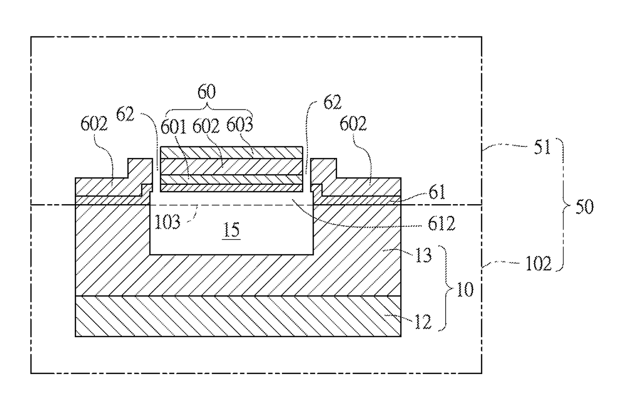
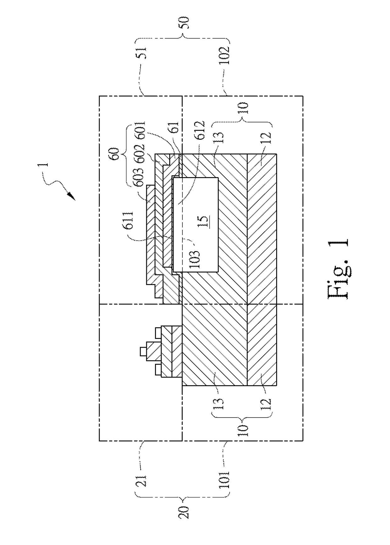
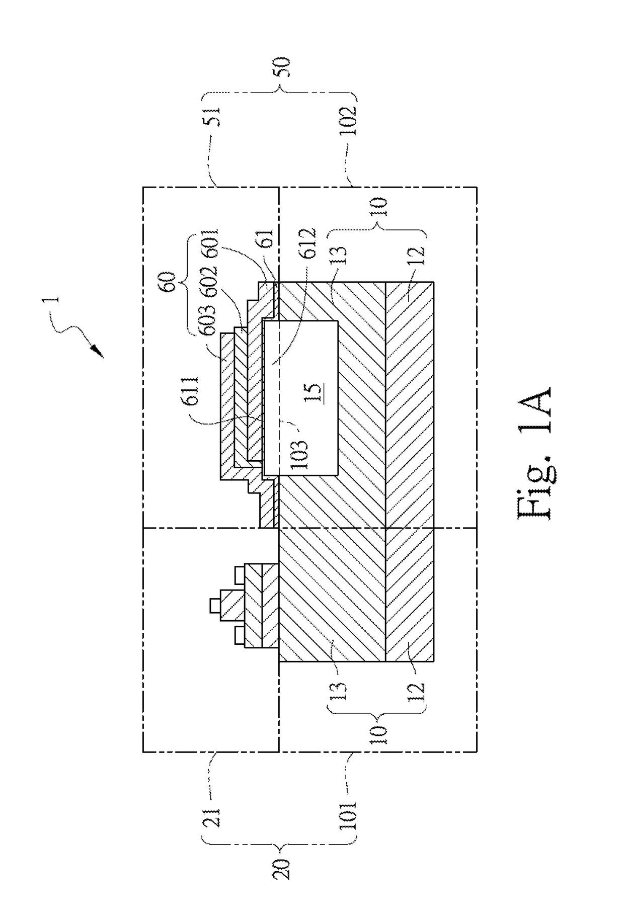
[0121]Please refer to FIG. 1, the cross-sectional view of an embodiment of the integrated structure of power amplifier and acoustic wave device of the present invention, the integrated structure comprises: a compound semiconductor epitaxial substrate 10, a power amplifier upper structure 21 and a film bulk acoustic resonator 51. The compound semiconductor epitaxial substrate 10 includes a compound semiconductor substrate 12 and an epitaxial structure 13 formed on the compound semiconductor substrate 12. The power amplifier upper structure 21 is formed on a first side 101 of the compound semiconductor epitaxial substrate 10, wherein the first side 101 of the compound semiconductor epitaxial substrate 10 and the power amplifier upper structure 21 form a power amplifier 20. The film bulk acoustic resonator 51 is formed on a second side 102 of the compound semiconductor epitaxial substrate 10, wherein the second side 102 of the compound semiconductor epitaxial substrate 10 and the film ...


PUM


Abstract

An integrated structure of acoustic wave device and varactor comprises an acoustic wave device and a varactor formed on a first part and a second part of a semiconductor substrate respectively. The acoustic wave device comprises an acoustic wave device upper structure and a first part of a bottom epitaxial structure. The acoustic wave device upper structure is formed on the first part of the bottom epitaxial structure. The varactor comprises a varactor upper structure and a second part of the bottom epitaxial structure. The varactor upper structure is formed on the second part of the bottom epitaxial structure. The integrated structure of the acoustic wave device and the varactor formed on the same semiconductor substrate is capable of reducing the module size, optimizing the impedance matching, and reducing the signal loss between the varactor and the acoustic wave device.

Description

CROSS-REFERENCE TO RELATED DOCUMENTS[0001]The present invention is a continuation in part (CIP) to a U.S. patent application Ser. No. 14 / 586,592 entitled “IMPROVED ACOUSTIC WAVE DEVICE STRUCTURE, INTEGRATED STRUCTURE OF POWER AMPLIFIER AND ACOUSTIC WAVE DEVICE, AND FABRICATION METHODS THEREOF” filed on Dec. 30, 2014.FIELD OF THE INVENTION[0002]The present invention relates to an integrated structure of power amplifier and acoustic wave device, wherein the integrated structure of the power amplifier and the acoustic wave device on the same compound semiconductor epitaxial substrate is capable of reducing the component size, optimizing the impedance matching, and reducing the signal loss between the power amplifier and the acoustic wave device.BACKGROUND OF THE INVENTION[0003]Please refer to FIG. 7˜7D, which are the schematics of conventional production processes of acoustic wave device. First, forming a recess 702 on a silicon substrate 701; then forming a protection layer 703 on the...

Claims


Application Information

Patent Timeline
Patent Type & Authority Applications(United States)
IPC IPC(8): H01L27/20H03H9/13H01L29/93H01L23/66H01L41/332H01L27/06H01L29/66H01L21/8252H03F3/213H03H9/17H01L29/20
CPCH01L27/20H03H9/171H03H9/13H01L29/93H01L23/66H01L2223/6655H01L27/0605H01L29/66174H01L21/8252H03F3/213H01L41/332H01L29/20H03H9/0542H03H9/173H10N39/00H10N30/071H03H9/02007
Inventor TSAI, SHU-HSIAOLIN, RE CHINGLIAO, PEI-CHUNLIN, CHENG-KUOCHIN, YUNG-CHUNG
Owner WIN SEMICON
Learn More