Electrostatic chuck

a technology of electrostatic chuck and chuck body, which is applied in the direction of electrostatic holding device, metal-working machine components, manufacturing tools, etc., can solve the problems of warpage in the electrostatic chuck, and achieve the effect of reducing temperature unevenness in the plane direction, reducing temperature unevenness in the attraction substrate, and reducing temperature unevenness in the attraction object such as a semiconductor wafer attracted to the attraction substra

Active Publication Date: 2017-05-11
NGK SPARK PLUG CO LTD
View PDF2 Cites 9 Cited by
  • Summary
  • Abstract
  • Description
  • Claims
  • Application Information

AI Technical Summary

Benefits of technology

[0048]Accordingly, even when the heating state is uneven (depending on the position of the heating element) due to the structure, arrangement, or the like of the heating element provided in the heater member, the anisotropic heat conductor allows heat to be transferred easier in the plane direction than in the thickness direction, whereby temperature unevenness in the plane direction is reduced.
[0049]Thus, temperature unevenness in the attraction substrate (i.e., temperature unevenness at the substrate surface in the plane direction) can be reduced. In other words, the temperature at the substrate surface in the plane direction can be made uniform.
[0050]Accordingly, temperature unevenness in the attraction object such as a semiconductor wafer attracted to the attraction substrate can be reduced. Thus, it is possible to reduce occurrence of a problem such as variation in the degree of processing in forming a pattern on a semiconductor wafer by plasma etching, for example. As a result, when processing an attraction object member, the yield can be improved.
[0051]Further, in this electrostatic chuck, the another heating element is configured to include a plurality of heating elements separately disposed at different positions in the plane direction so that the temperature of the attraction substrate can be controlled to different temperatures depending on the positions in the plane direction. Therefore, by controlling the temperatures of the plurality of heating elements to desired temperatures, the temperature of the attraction substrate can be controlled to different temperatures depending on the positions in the plane direction.
[0052]That is, when there is a demand (challenge) to control the temperature of the attraction substrate (consequently, the attraction object member) in the plane direction to be varied depending on positions, the temperature of the attraction object member can be easily controlled to desired different temperatures in the plane direction by controlling the temperatures of the separated heating elements as in this electrostatic chuck.

Problems solved by technology

Besides, in the electrostatic chuck having the above-mentioned structure, since the ceramic insulating plate and the metal base have difference thermal expansion coefficients, when the temperature changes, warpage may occur in the electrostatic chuck due to a thermal stress generated between the ceramic insulating plate and the metal base.

Method used


Image

  • Electrostatic chuck
  • Electrostatic chuck
  • Electrostatic chuck

Examples


embodiment 1

[0118]In this embodiment, an electrostatic chuck capable of attracting and holding, for example, a semiconductor wafer is exemplified.

[0119]a) First, the structure of the electrostatic chuck according to Embodiment 1 will be described.

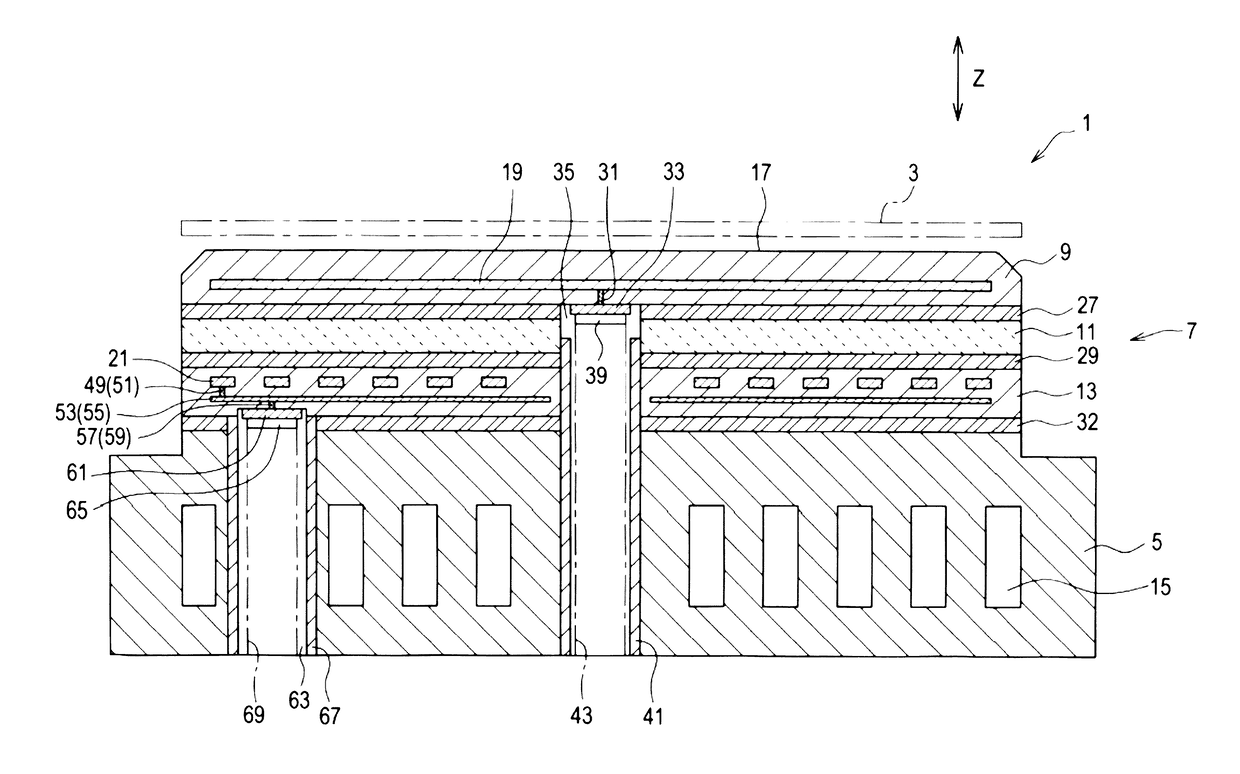
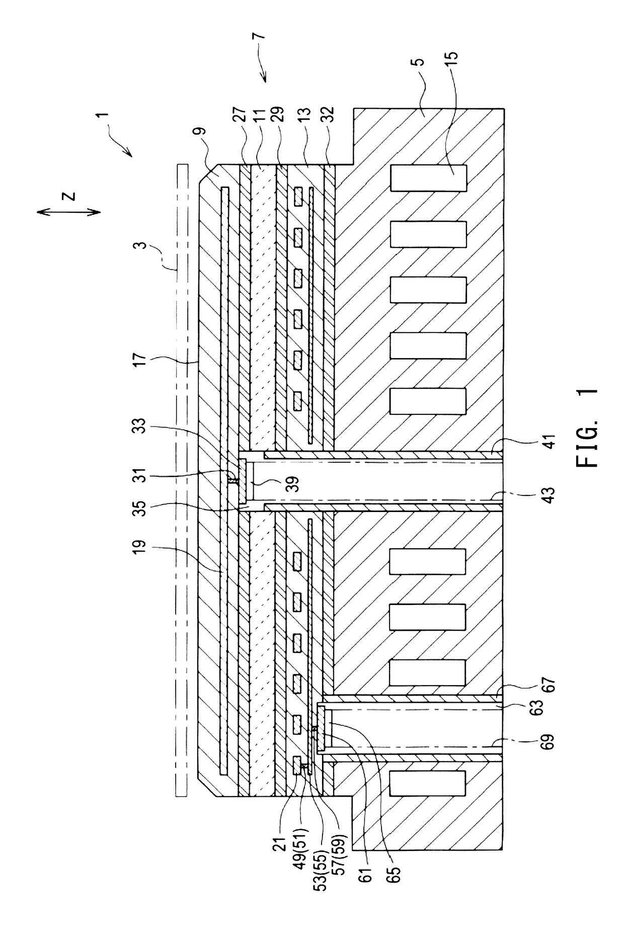
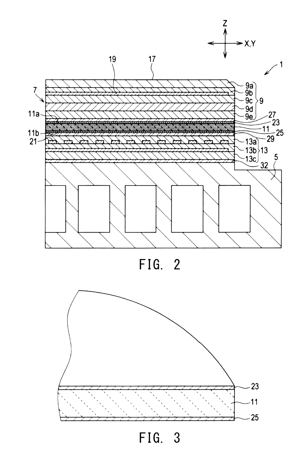
[0120]As schematically shown in FIG. 1, the electrostatic chuck 1 according to Embodiment 1 is a device for attracting a semiconductor wafer 3 at its front side (attraction side: upper side in FIG. 1). This electrostatic chuck 1 is obtained by adhering a disk-like attraction member 7 having, for example, a diameter of 300 mm and a thickness of 3 mm for attracting the semiconductor wafer 3, onto one side (upper side in FIG. 1), in the thickness direction, of a disk-like metal base (cooling plate) 5 having, for example, a diameter of 340 mm and a thickness of 20 mm.

[0121]The thickness direction is the up-down direction in FIG. 1 (stacking direction: Z direction), and a direction perpendicular to the thickness direction is a direction (plane direction: pl...

embodiment 2

[0189]Next, Embodiment 2 will be described. Description of components similar to those of Embodiment 1 will be omitted.

[0190]Embodiment 2 is greatly different from Embodiment 1 in that another heater member (hereinafter referred to as a second heater member) is disposed between the attraction substrate and the graphite sheet.

[0191]a) First, the schematic structure of the electrostatic chuck according to Embodiment 2 will be described.

[0192]As schematically shown in FIG. 8, the electrostatic chuck 81 according to Embodiment 2 includes an attraction member 83 and a metal base 85 as in Embodiment 1.

[0193]As in Embodiment 1, the attraction member 83 includes an attraction substrate 87, a graphite sheet 89 (anisotropic heat conductor), and a first heater member 91, and further includes a disk-like (in a plan view) second heater member 93 disposed between the attraction substrate 87 and the graphite sheet 89.

[0194]Specifically, as shown in FIG. 9, the attraction substrate 87 is composed o...


PUM

PropertyMeasurementUnit
thicknessaaaaaaaaaa
heat resistanceaaaaaaaaaa
thicknessaaaaaaaaaa

Abstract

An electrostatic chuck includes an anisotropic heat conductor which is disposed between an attraction substrate and a first heater member, and has an upper surface and a lower surface, and a coefficient of thermal conductivity which varies depending on directions. The anisotropic heat conductor is disposed so that the coefficient of thermal conductivity in a plane direction is larger than the coefficient of thermal conductivity in a thickness direction. Further, the electrostatic chuck includes metal layers which are joined to the anisotropic heat conductor so as to cover the upper surface and the lower surface of the anisotropic heat conductor, and an adhesive layer which is provided on a surface of each metal layer, and joins the metal layer to the attraction substrate or the heater member. Moreover, at least one of the metal layers is a fused metal layer formed by solidifying a melted metal.

Description

CROSS REFERENCE TO RELATED PATENT APPLICATIONS[0001]This international application claims priority to Japanese Patent Application No. 2014-128315 filed Jun. 23, 2014 in the Japanese Patent Office, which is incorporated herein by reference in its entirety.TECHNICAL FIELD[0002]The present invention relates to an electrostatic chuck used for fixing of a semiconductor wafer, adjustment of flatness of a semiconductor wafer, and the like, for example.BACKGROUND ART[0003]Conventionally, a semiconductor manufacturing apparatus performs processing such as dry etching (for example, plasma etching) on a semiconductor wafer (for example, silicon wafer). In order to enhance accuracy of the dry etching, the semiconductor wafer needs to be reliably fixed. As fixing means for fixing a semiconductor wafer, an electrostatic chuck which fixes a semiconductor wafer by means of an electrostatic attraction force has been proposed (refer to Patent Document 1, for example).[0004]Specifically, an electrosta...

Claims


Application Information

Patent Timeline
Patent Type & Authority Applications(United States)
IPC IPC(8): H01L21/683H01L21/67
CPCH01L21/67103H01L21/6833H01L21/6831H01L21/68757H01L21/68785B23Q3/15H01L21/324H02N13/00
Inventor MIWA, KANAMESAITO, SHOTA
Owner NGK SPARK PLUG CO LTD
Why Eureka
Try Eureka