
Organic light emitting display device and method of fabricating the same

a technology of light-emitting display device and organic material, which is applied in the direction of organic semiconductor device, sustainable manufacturing/processing, final product manufacturing, etc., can solve the problems of high power consumption, and low luminous efficiency and brightness of plasma display device, so as to prevent moisture permeation

Active Publication Date: 2017-03-23
LG DISPLAY CO LTD
View PDF1 Cites 16 Cited by
  • Summary
  • Abstract
  • Description
  • Claims
  • Application Information

AI Technical Summary

Benefits of technology

This method effectively prevents the permeation of moisture and foreign materials, enhancing the reliability and lifespan of the organic light emitting display devices by eliminating cracks in the passivation layer during the cutting process.

Problems solved by technology

However, the plasma display device also has disadvantages in view of low luminous efficiency and brightness and high power consumption.
On the other hand, the LCD device has disadvantages in view of being difficult to implement a large screen due to the use of a semiconductor process and causing high power consumption due to a backlight unit.
Also, the LCD device exhibits a great optical loss and a narrow viewing angle due to optical elements, such as a polarizing filter, a prism sheet, a diffusion plate and the like.
The inorganic light emitting display device causes high power consumption and is unable to obtain high brightness, as compared with the organic light emitting display device.
Due to the permeation of the impurities such as moisture or air, a defective organic light emitting display device is fabricated and a lifespan of the device is reduced.

Method used


Image

  • Organic light emitting display device and method of fabricating the same
  • Organic light emitting display device and method of fabricating the same
  • Organic light emitting display device and method of fabricating the same

Examples


Embodiment Construction

[0022]Description will now be given in detail of the exemplary embodiments, with reference to the accompanying drawings. For the sake of brief description with reference to the drawings, the same or equivalent components will be provided with the same reference numbers, and description thereof will not be repeated.

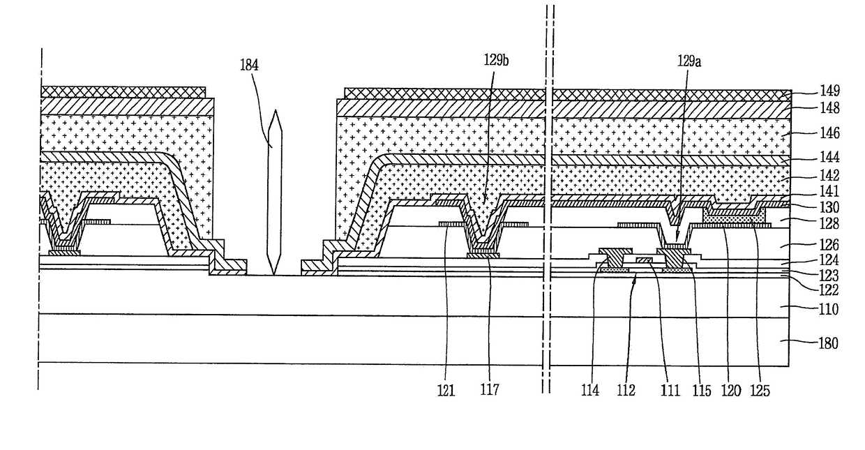
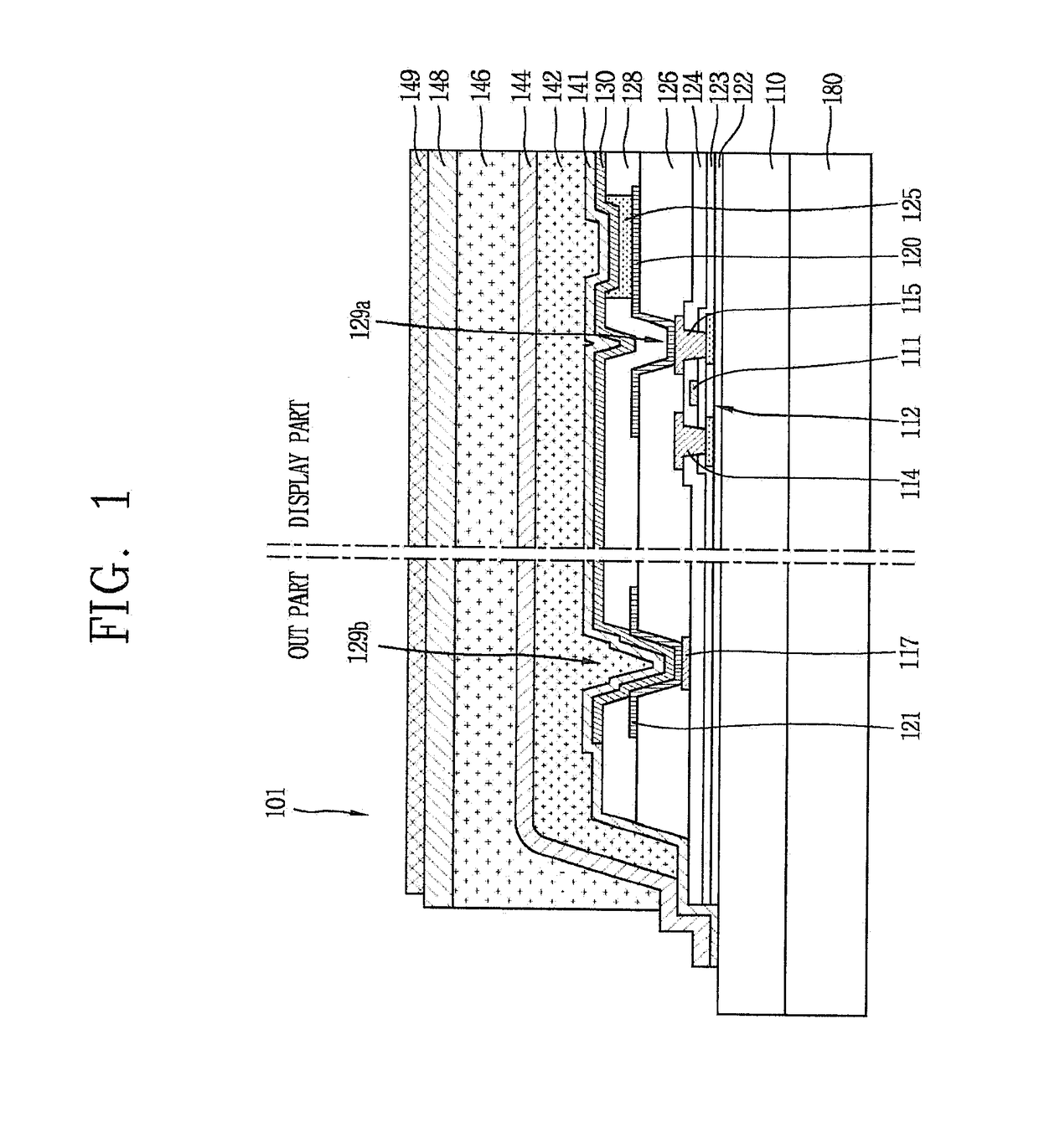
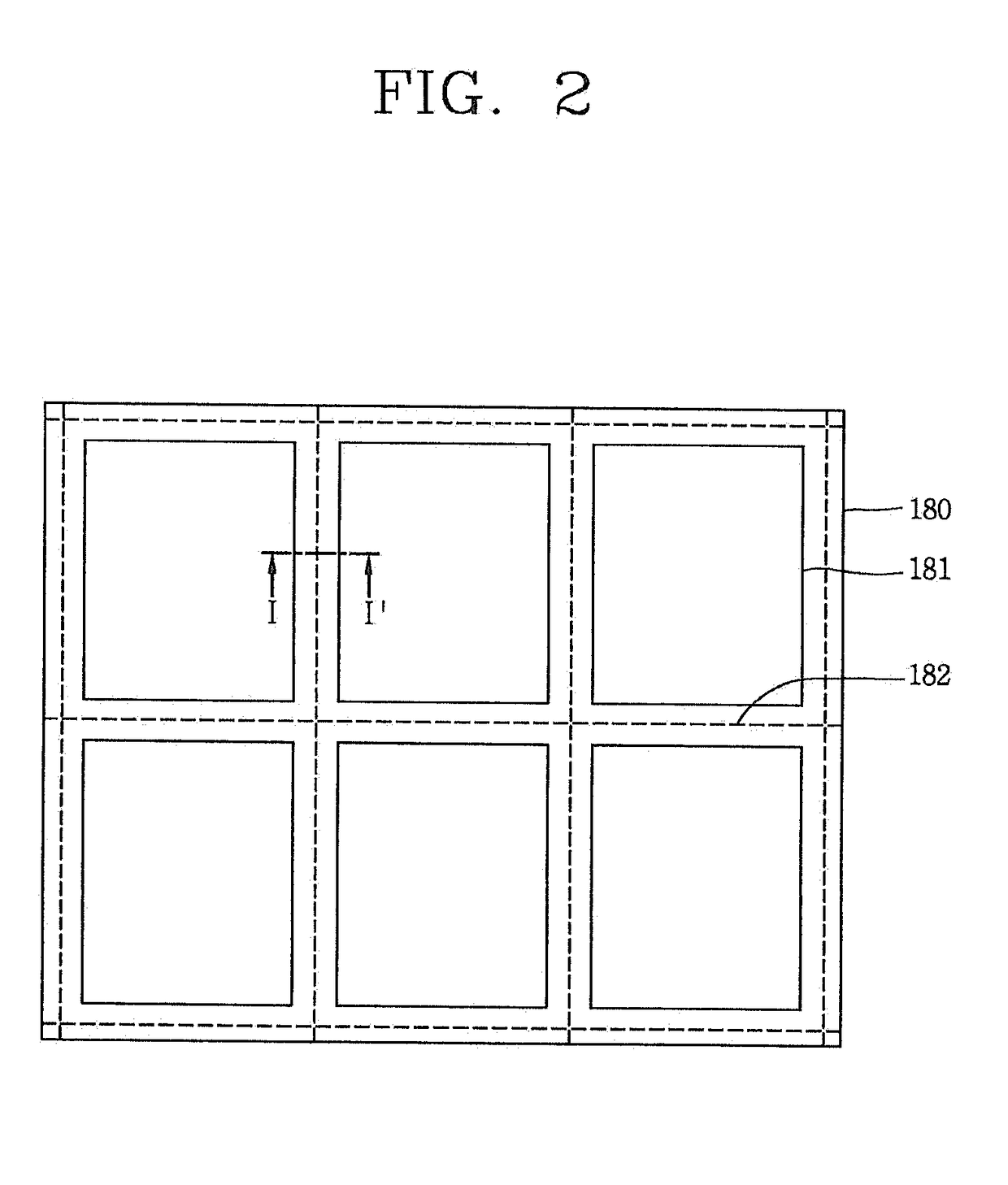
[0023]In an organic light emitting display device according to the present disclosure, upon forming a plurality of display panels on a large mother substrate, various electrodes and light emitting layers may be formed on a flexible plastic substrate, without forming a passivation layer on a region between the adjacent display panels. This may prevent a production of cracks on the passivation layer during a cutting process of cutting the mother substrate, which may result in prevention of permeation of moisture or foreign materials through the cracks.

[0024]FIG. 1 is a view of a structure of an organic light emitting display device in accordance with the present disclosure. ...


PUM


Abstract

The present disclosure relates to an organic light emitting display device including a substrate having an outer part and a display part, a driving thin film transistor on each of a plurality of pixel regions within the display part of the substrate, a pixel electrode on each pixel region of the display part, an organic light emitting unit on each pixel region of the display part to emit light, a common electrode on the organic light emitting unit and a bank layer to apply a signal to the organic light emitting layer, and a first passivation layer, an organic insulating layer and a second passivation layer on the outer part and the display part, wherein the first passivation layer and the second passivation layer are removed from the outermost region of the outer part, so that the substrate is exposed to the outside.

Description

CROSS-REFERENCE TO RELATED APPLICATION[0001]This is a Divisional of U.S. patent application Ser. No. 14 / 065,677, filed on Oct. 29, 2013, which claims the benefit of Korean Patent Application No. 10-2012-0122699, filed on Oct. 31, 2012, both of which are hereby incorporated by reference for all purposes as if fully set forth herein.BACKGROUND OF THE DISCLOSURE[0002]1. Field of the Disclosure[0003]This specification relates to an organic light emitting display device and a fabricating method thereof, and more particularly, to an organic light emitting display device capable of preventing an occurrence of deterioration or defect due to permeation of air or moisture through cracks formed on a passivation layer, and a fabricating method thereof.[0004]2. Background of the Disclosure[0005]In recent time, various types of flat panel display devices capable of reducing weights and volumes, which are disadvantages of a cathode ray tube, are being developed. Examples of the flat panel display ...

Claims


Application Information

Patent Timeline
Patent Type & Authority Applications(United States)
IPC IPC(8): H01L51/56H01L51/00H01L51/52H10N10/856
CPCH01L51/56H01L51/5253H01L2251/566H01L2227/323H01L27/3244H01L51/0097Y02E10/549Y02P70/50H10K71/851H10K59/8731H10K59/12H10K59/873H01L27/1244H01L27/1262H05B33/04H10K59/1201H10K71/00H10K50/844H10K77/111
Inventor KWON, JUNYOUNGKIM, SUNGHUNKIM, MISO
Owner LG DISPLAY CO LTD
Learn More