Diamond components for quantum imaging, sensing and information processing devices

a quantum imaging and sensing technology, applied in the direction of crystal growth process, polycrystalline material growth, chemically reactive gas, etc., can solve the problems of negate the requirement for expensive and bulky cryogenic cooling apparatus, defects exhibit a shorter spin coherence time, etc., to achieve low surface roughness, long spin coherence time, and low surface damage

Active Publication Date: 2016-12-01
ELEMENT SIX TECH LTD
View PDF2 Cites 56 Cited by
  • Summary
  • Abstract
  • Description
  • Claims
  • Application Information

AI Technical Summary

Benefits of technology

The patent describes a method for creating nitrogen-vacancy defects in diamond material by implanting nitrogen into an as-grown growth face of a single crystal CVD diamond layer without any polishing or etching of the surface. This results in near surface nitrogen-vacancy defects with longer spin coherence times compared to those formed on a polished or etched surface. The method also allows for the formation of smooth surfaces with minimal damage, which can be patterned for use in sensing and quantum processing applications. This results in a single crystal CVD diamond component with near surface nitrogen-vacancy defects that provide long spin coherence times for various applications such as nanomagnetometry and quantum information processing.

Problems solved by technology

This can negate the requirement for expensive and bulky cryogenic cooling apparatus for certain applications where miniaturization is desired.
One problem with the formation of near surface NV− defects in synthetic diamond materials via nitrogen ion implantation and annealing is that to date such near surface NV− defects exhibit a shorter spin coherence time than native NV− defects found in the bulk of high purity single crystal CVD diamond material such as the single crystal CVD diamond materials described in WO01 / 096633, WO2010 / 010344, and WO2010 / 010352.

Method used


Image

  • Diamond components for quantum imaging, sensing and information processing devices
  • Diamond components for quantum imaging, sensing and information processing devices
  • Diamond components for quantum imaging, sensing and information processing devices

Examples


Embodiment Construction

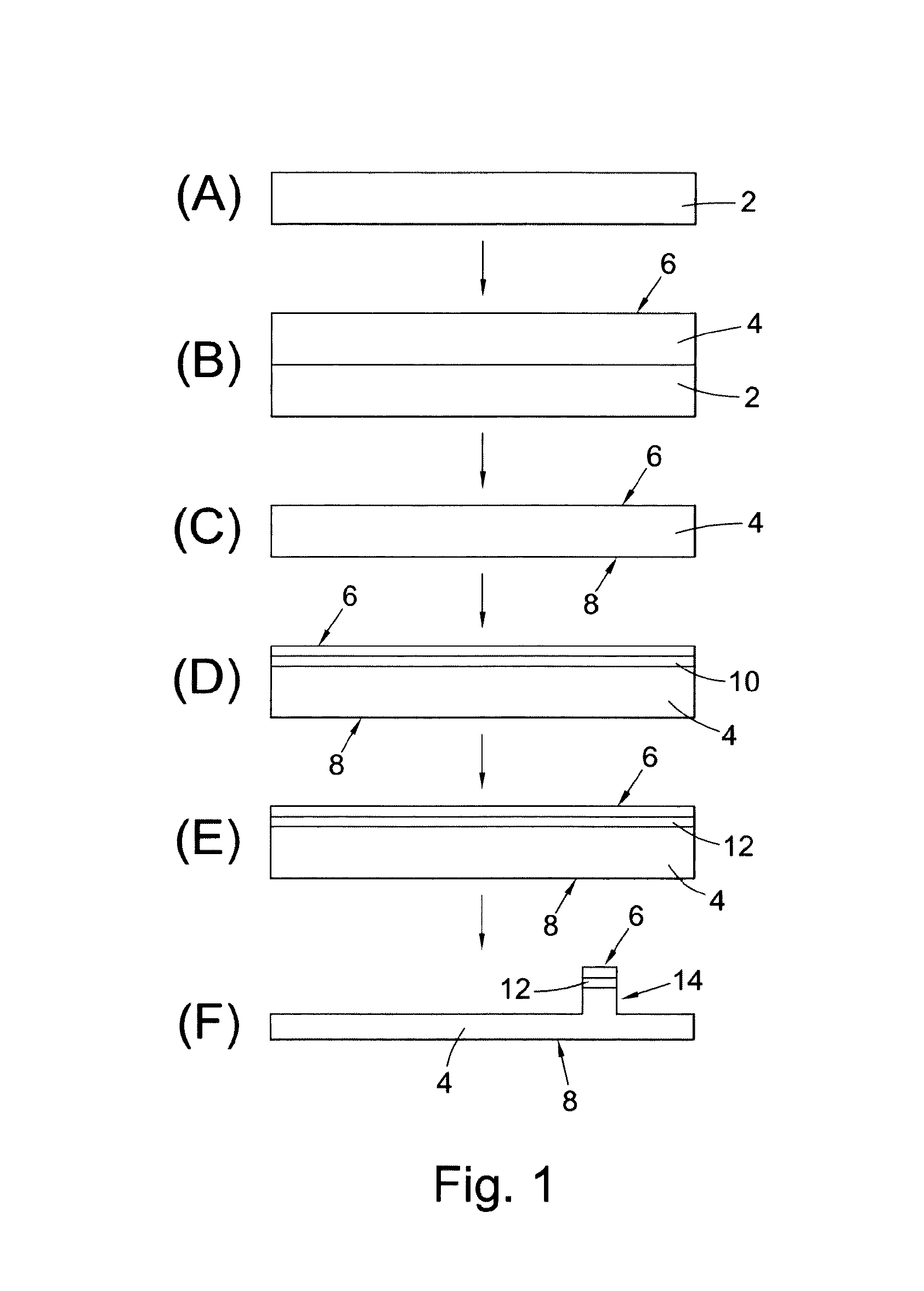
[0042]As described in the summary of invention section, a method of fabricating a diamond component is provided for a quantum imaging, sensing, or information processing device, the method comprising:

[0043]growing a single crystal CVD diamond layer having an as-grown growth face, at least a portion of the as-grown growth face having a surface roughness Ra of no more than 100 nm;

[0044]implanting nitrogen into said as-grown growth face of the single crystal CVD diamond layer without any polishing or etching of the as-grown growth face; and

[0045]annealing the single crystal CVD diamond layer to cause migration of vacancy and / or nitrogen defects within the single crystal CVD diamond layer and formation of nitrogen-vacancy defects from the implanted nitrogen and the vacancy defects.

[0046]FIG. 1 illustrates the aforementioned method. The starting point (FIG. 1A) is a single crystal diamond substrate 2 which is suitably prepared for single crystal CVD diamond growth thereon.

[0047]Next (FIG...


PUM

PropertyMeasurementUnit
Lengthaaaaaaaaaa
Fractionaaaaaaaaaa
Fractionaaaaaaaaaa

Abstract

A single crystal CVD diamond component comprising: a surface, wherein at least a portion of said surface is formed of as-grown growth face single crystal CVD diamond material which has not been polished or etched and which has a surface roughness Ra of no more than 100 nm; and a layer of NV− defects, said layer of NV− defects being disposed within 1 μm of the surface, said layer of NV− defects having a thickness of no more than 500 nm, and said layer of NV− defects having a concentration of NV− defects of at least 105 NV− / cm2.

Description

FIELD OF INVENTION[0001]The present invention relates to diamond components for quantum imaging, sensing, and information processing devices and to methods of fabricating single crystal chemical vapour deposited (CVD) diamond components for use in quantum imaging, sensing, and information processing applications.BACKGROUND OF INVENTIOn[0002]Point defects in synthetic diamond material, particularly quantum spin defects and / or optically active defects, have been proposed for use in various imaging, sensing, and processing applications including: luminescent tags; magnetometers; spin resonance devices such as nuclear magnetic resonance (NMR) and electron spin resonance (ESR) devices; spin resonance imaging devices for magnetic resonance imaging (MRI); and quantum information processing devices such as for quantum communication and computing.[0003]Many point defects have been studied in synthetic diamond material including: silicon containing defects such as silicon-vacancy defects (Si—...

Claims


Application Information

Patent Timeline
IPC IPC(8): C30B31/22H01L21/04C30B29/68H01L29/16C30B25/20C30B29/04
CPCC30B31/22C30B25/20H01L21/042C30B29/68H01L29/1602C30B29/04C30B25/186C30B25/205C23C16/27C01B32/25
Inventor MARKHAM, MATTHEWSTACEY, ALASTAIRTWITCHEN, DANIEL
Owner ELEMENT SIX TECH LTD
Why Eureka
Try Eureka