
LOW DEFECT RELAXED SiGe/STRAINED Si STRUCTURES ON IMPLANT ANNEAL BUFFER/STRAIN RELAXED BUFFER LAYERS WITH EPITAXIAL RARE EARTH OXIDE INTERLAYERS AND METHODS TO FABRICATE SAME

a rare earth oxide and buffer layer technology, applied in the direction of semiconductor devices, electrical equipment, basic electric elements, etc., can solve the problems of metal oxide semiconductor transistors that are beginning to reach their traditional scaling limits and high defect density that can be presen

Active Publication Date: 2016-11-03
IBM CORP
View PDF3 Cites 4 Cited by
  • Summary
  • Abstract
  • Description
  • Claims
  • Application Information

AI Technical Summary

Benefits of technology

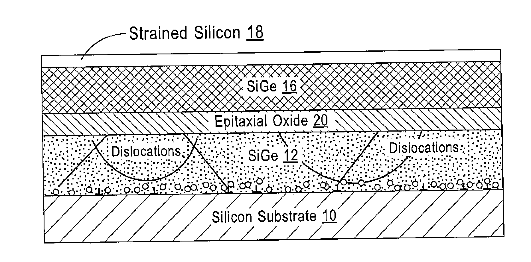
This patent describes a structure that includes two layers of semiconductor material that have different geometries to prevent misfit dislocations from spreading from one layer to the next. The structure also includes a layer of metal-containing oxide that helps to stabilize the semiconductor layers. Overall, this structure helps to create a more stable and high-quality semiconductor device.

Problems solved by technology

However, there are growing signs today that metal oxide semiconductor transistors are beginning to reach their traditional scaling limits.
However, a problem that can arise with respect to this fabrication process relates to a high defect density that can be present at the surface of the IAB / SRB layer.

Method used


Image

  • LOW DEFECT RELAXED SiGe/STRAINED Si STRUCTURES ON IMPLANT ANNEAL BUFFER/STRAIN RELAXED BUFFER LAYERS WITH EPITAXIAL RARE EARTH OXIDE INTERLAYERS AND METHODS TO FABRICATE SAME
  • LOW DEFECT RELAXED SiGe/STRAINED Si STRUCTURES ON IMPLANT ANNEAL BUFFER/STRAIN RELAXED BUFFER LAYERS WITH EPITAXIAL RARE EARTH OXIDE INTERLAYERS AND METHODS TO FABRICATE SAME
  • LOW DEFECT RELAXED SiGe/STRAINED Si STRUCTURES ON IMPLANT ANNEAL BUFFER/STRAIN RELAXED BUFFER LAYERS WITH EPITAXIAL RARE EARTH OXIDE INTERLAYERS AND METHODS TO FABRICATE SAME

Examples


Embodiment Construction

[0014]The word “exemplary” is used herein to mean “serving as an example, instance, or illustration.” Any embodiment described herein as “exemplary” is not necessarily to be construed as preferred or advantageous over other embodiments. All of the embodiments described in this Detailed Description are exemplary embodiments provided to enable persons skilled in the art to make or use the invention and not to limit the scope of the invention which is defined by the claims.

[0015]The terms “epitaxial growth and / or deposition” and “epitaxially formed and / or grown” mean the growth of a semiconductor material on a deposition surface of a semiconductor material, in which the semiconductor material being grown has the same crystalline characteristics as the semiconductor material of the deposition surface. In an epitaxial deposition process, the chemical reactants provided by source gases are controlled and the system parameters are set so that the depositing atoms arrive at the deposition s...


PUM


Abstract

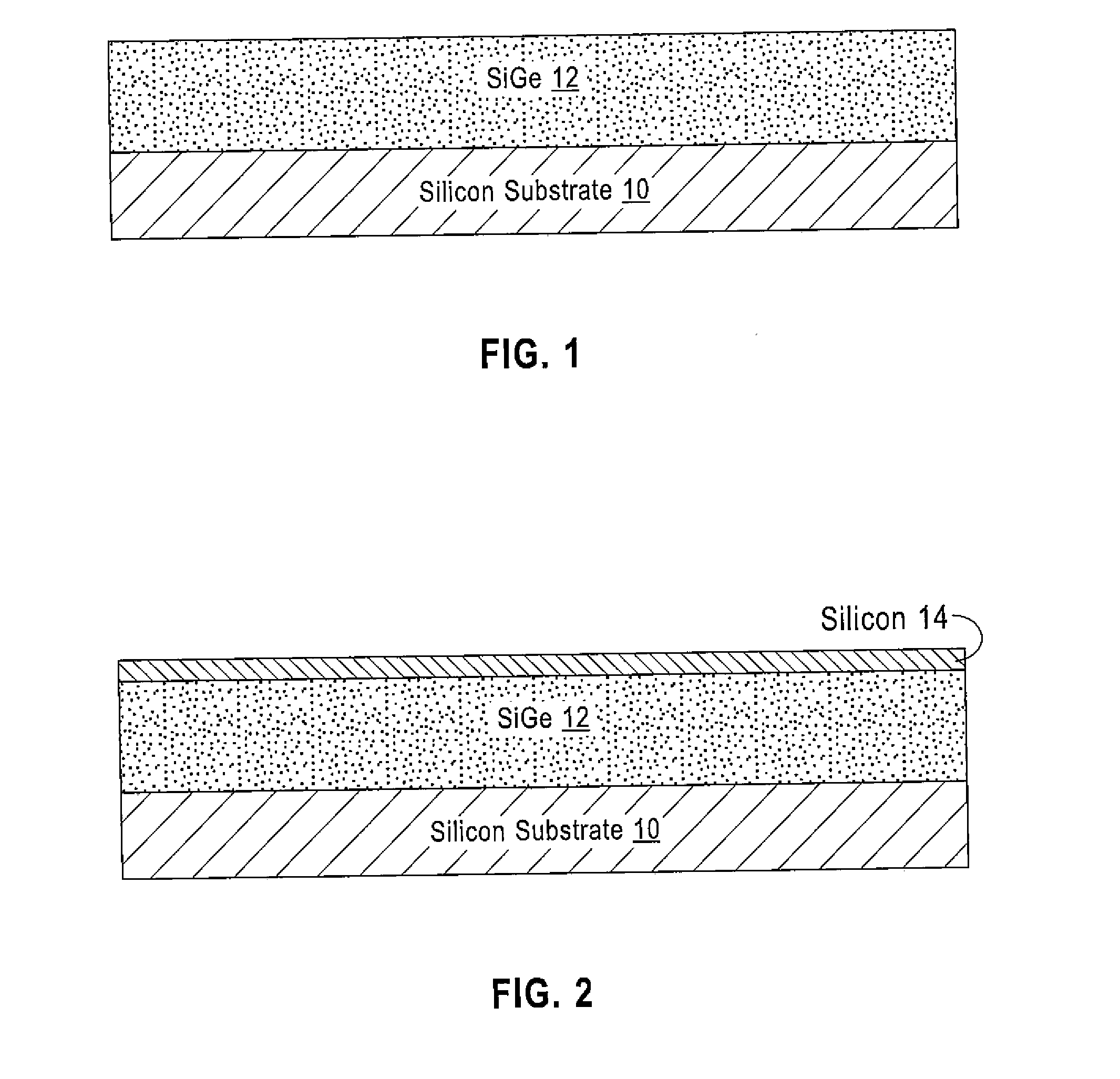
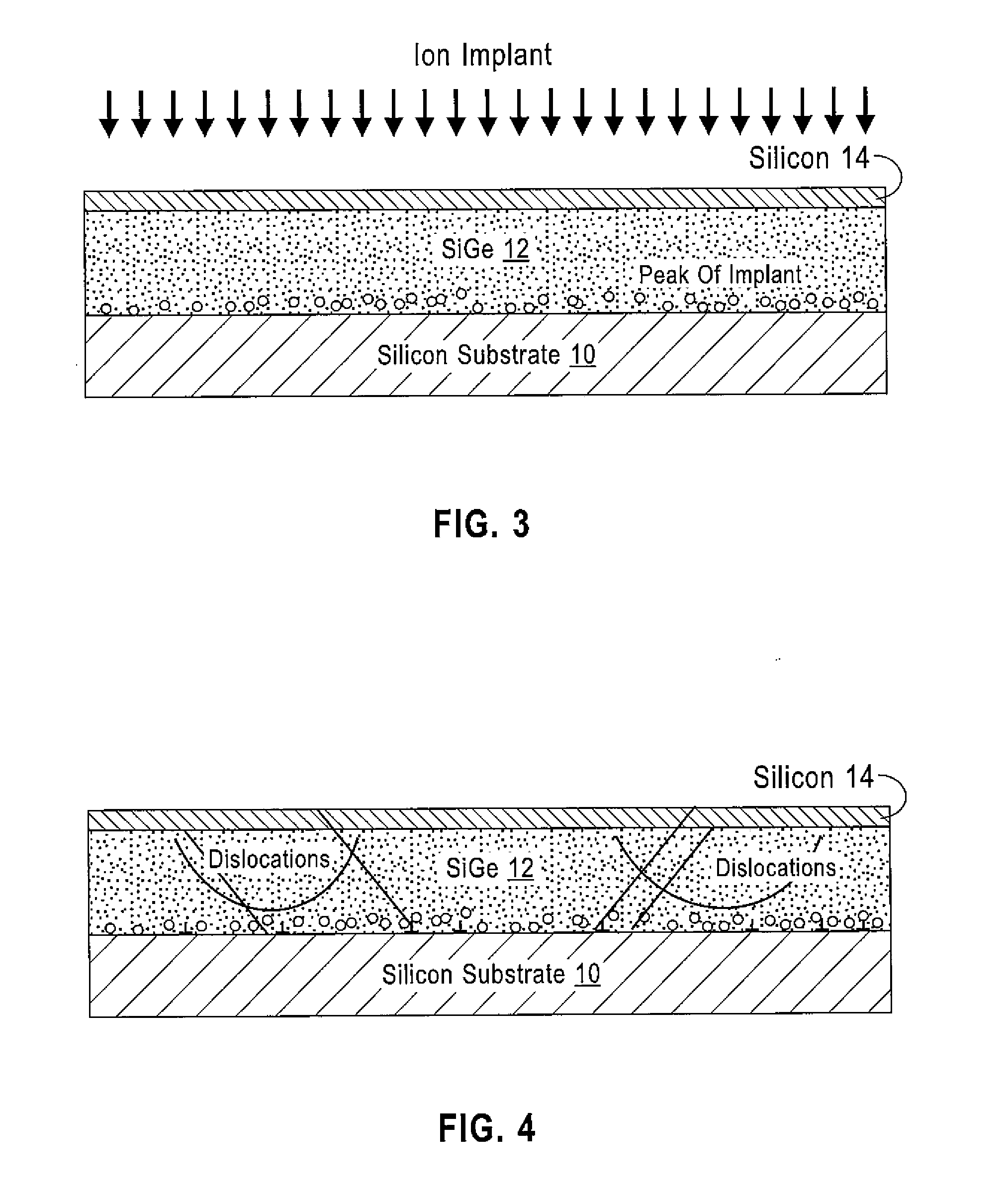
A method provides a substrate having a top surface; forming a first semiconductor layer on the top surface, the first semiconductor layer having a first unit cell geometry; epitaxially depositing a layer of a metal-containing oxide on the first semiconductor layer, the layer of metal-containing oxide having a second unit cell geometry that differs from the first unit cell geometry; ion implanting the first semiconductor layer through the layer of metal-containing oxide; annealing the ion implanted first semiconductor layer; and forming a second semiconductor layer on the layer of metal-containing oxide, the second semiconductor layer having the first unit cell geometry. The layer of metal-containing oxide functions to inhibit propagation of misfit dislocations from the first semiconductor layer into the second semiconductor layer. A structure formed by the method is also disclosed.

Description

TECHNICAL FIELD[0001]The embodiments of this invention relate generally to semiconductor devices and fabrication techniques and, more specifically, relate to the fabrication of semiconductor transistor devices.BACKGROUND[0002]For more than three decades, the continued miniaturization of metal oxide semiconductor field effect transistors (MOSFETs) has driven the worldwide semiconductor industry. Various impediments to continued scaling have been predicted for decades, but a history of innovation has sustained Moore's Law in spite of many challenges. However, there are growing signs today that metal oxide semiconductor transistors are beginning to reach their traditional scaling limits. Since it has become increasingly difficult to improve MOSFETs and therefore complementary metal oxide semiconductor (CMOS) performance through continued scaling, the development of further methods for improving performance, in addition to scaling, has become critical. One such method involves providing...

Claims


Application Information

Patent Timeline
IPC IPC(8): H01L21/02H01L29/165H01L29/32H01L29/04H01L21/265H01L21/324
CPCH01L21/02532H01L21/02488H01L21/02192H01L21/26506H01L29/165H01L21/02194H01L29/32H01L29/04H01L21/324H01L21/02381H01L21/0245H01L21/02483H01L21/02505H01L21/02694H01L29/1054H01L29/161H01L29/66795H01L21/02516H01L29/167
Inventor REZNICEK, ALEXANDER
Owner IBM CORP
Learn More