Amoled pixel driving circuit

Inactive Publication Date: 2016-10-20
TCL CHINA STAR OPTOELECTRONICS TECH CO LTD
View PDF4 Cites 14 Cited by
  • Summary
  • Abstract
  • Description
  • Claims
  • Application Information

AI Technical Summary

Benefits of technology

The present invention provides an AMOLED pixel driving circuit to solve the problem of unnecessary irradiance of the organic light emitting diode (OLED) during the process of compensating the drift of the threshold voltage of the drive thin film transistor. By adding a thin film transistor controlled by an irradiance control signal between the OLED and the power supply voltage or utilizing alternating current power supply voltage, the OLED can be turned off in the irradiance unnecessary period, extending the lifetime of the OLED and optimizing the actual display effect of the panel.

Problems solved by technology

In the AMOLED driving circuit, the threshold voltage of the drive thin film transistor will drift along with the working times. Thus, it results in that the luminescence of the OLED is unstable.
However, what the panel needs is that the organic light emitting diode OLED emits light only in the drive stage.
Such unnecessary irradiance will influence the lifetime of the OLED, and meanwhile will affect the actual display effect of the panel, such as the contrast ratio reduction, the appearance of the light leakage phenomenon, etc.

Method used


Image

  • Amoled pixel driving circuit
  • Amoled pixel driving circuit
  • Amoled pixel driving circuit

Examples


first embodiment

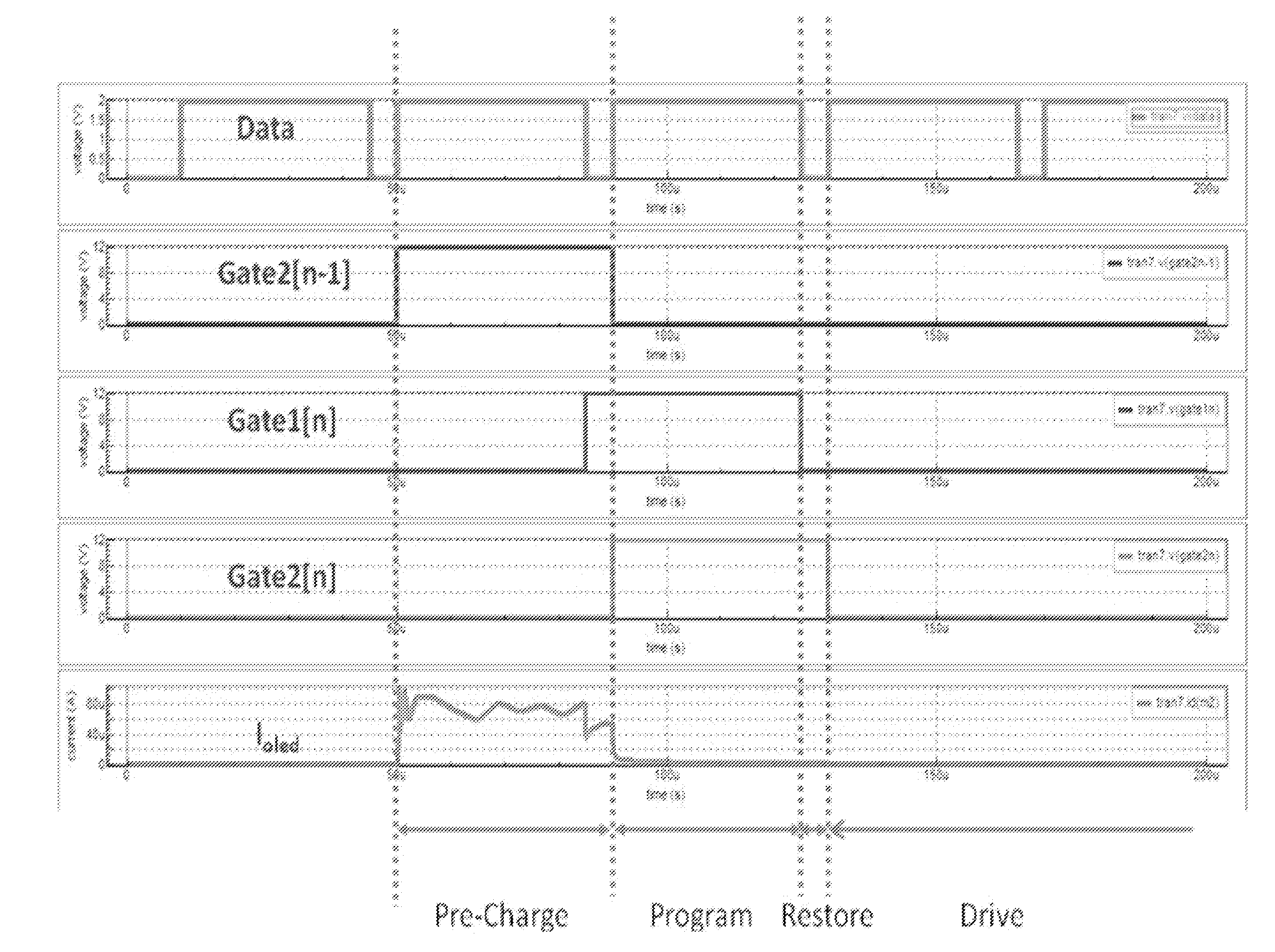
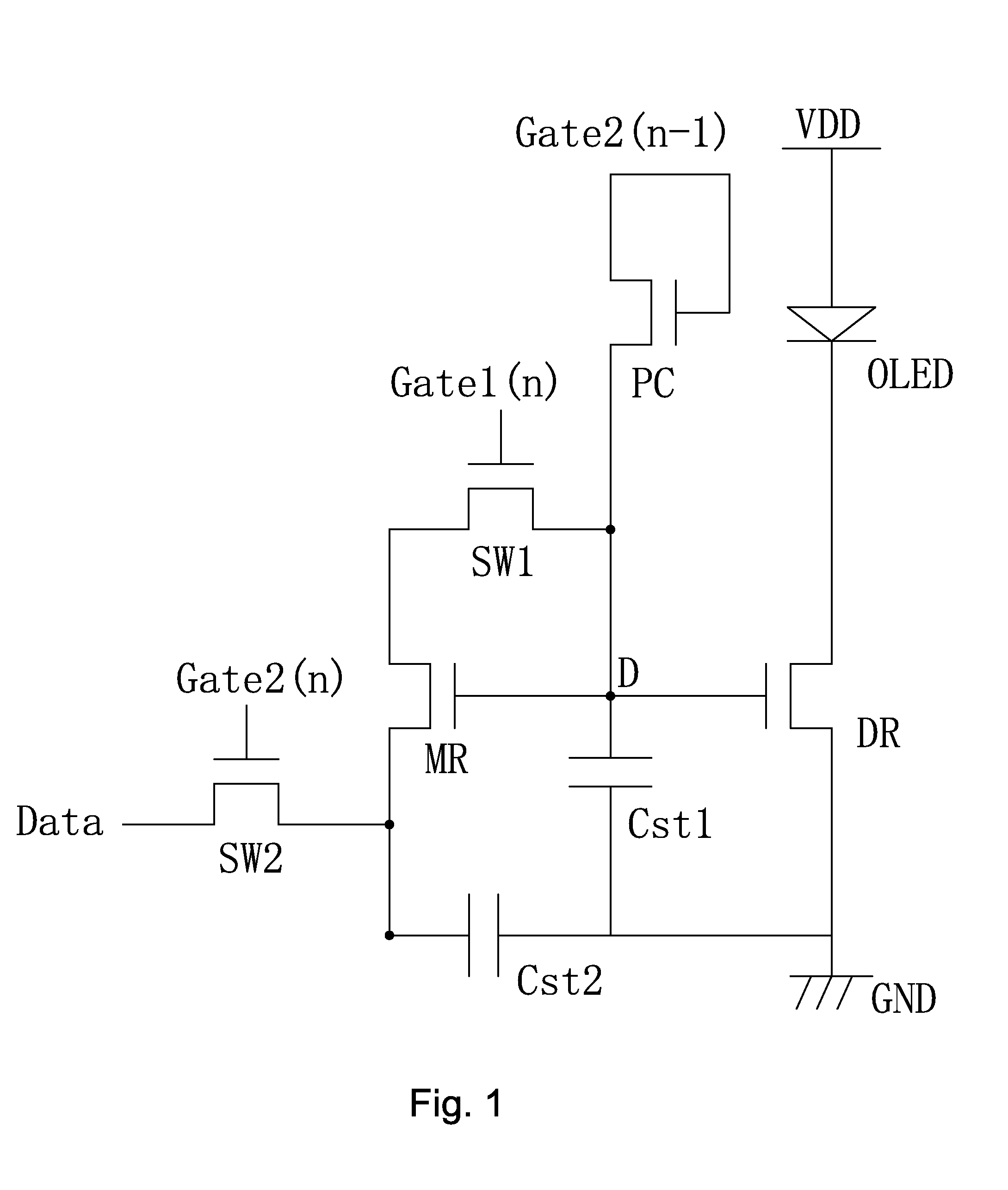
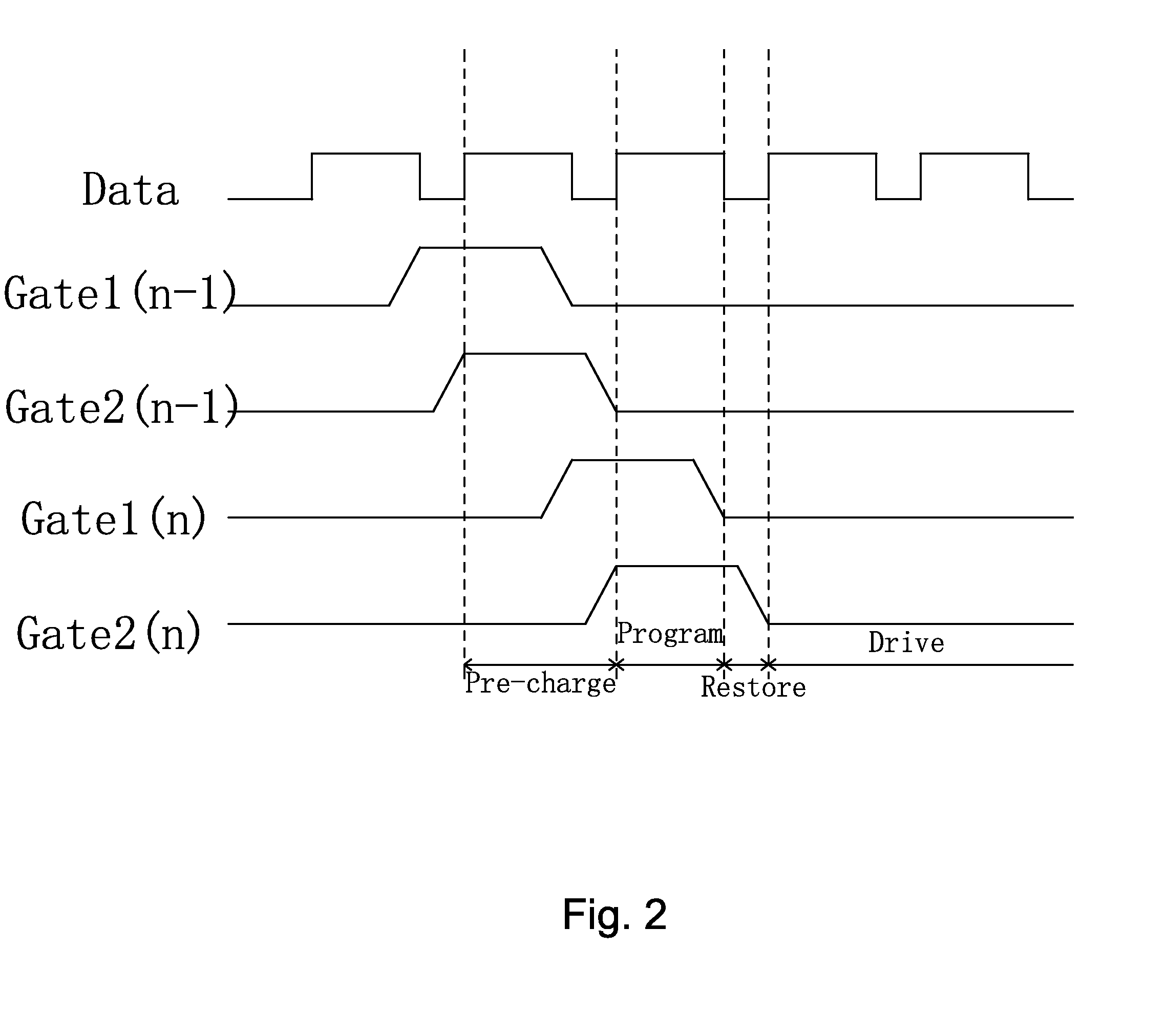
[0073]FIG. 4 shows the circuit diagram of the AMOLED pixel driving circuit according to the present invention, comprising: a first thin film transistor M1, a second thin film transistor M2, a third thin film transistor M3, a fourth thin film transistor M4, a fifth thin film transistor M5, a sixth thin film transistor M6, a first capacitor C1, a second capacitor C2 and an organic light emitting light diode D1. A gate of the sixth thin film transistor M6 is electrically coupled to an nth stage second scan control signal Gate2(n), and a source is electrically coupled to a data signal Data, and a drain is electrically coupled to a drain of the third thin film transistor M3 and one end of the first capacitor C1; a gate of the third thin film transistor M3 is electrically coupled to a gate of the fourth thin film transistor M4 via a first node D, and a source is electrically coupled to the source of the first thin film transistor M1, and the drain is electrically coupled to the drain of t...

second embodiment

[0078]FIG. 8. shows the circuit diagram of the AMOLED pixel driving circuit according to the present invention, comprising: a first thin film transistor M1, a third thin film transistor M3, a fourth thin film transistor M4, a fifth thin film transistor M5, a sixth thin film transistor M6, a first capacitor C1, a second capacitor C2 and an organic light emitting light diode D1. A gate of the sixth thin film transistor M6 is electrically coupled to an nth stage second scan control signal Gate2(n), and a source is electrically coupled to a data signal Data, and a drain is electrically coupled to a drain of the third thin film transistor M3 and one end of the first capacitor C1; a gate of the third thin film transistor M3 is electrically coupled to a gate of the fourth thin film transistor M4 via a first node D, and a source is electrically coupled to the source of the first thin film transistor M1, and the drain is electrically coupled to the drain of the sixth thin film transistor M6 ...


PUM


Abstract

The AMOLED pixel driving circuit provided by the present invention, by adding the thin film transistor (M2) controlled by the irradiance control signal (EM) between the organic light emitting diode (D1) and the direct current power supply voltage (VDD) or by utilizing the alternating current power supply voltage (VDD) to control whether the organic light emitting diode (D1) emits light or not to set the irradiance control signal (EM) or the alternating current power supply voltage (VDD) to provide high voltage level only in the drive stage and to provide low voltage level in the rest stages, makes the OLED to be in off state in the irradiance unnecessary period and stops the OLED emitting light in the irradiance unnecessary period. Thus, the issue that the unnecessary irradiance of the organic light emitting diode occurs during the process of compensating the drift of the threshold voltage of the drive thin film transistor in the AMOLED pixel driving circuit according to prior art can be solved to extend the lifetime of the OLED and optimize the actual display effect of the panel.

Description

FIELD OF THE INVENTION[0001]The present invention relates to a display technology field, and more particularly to an AMOLED pixel driving circuit.BACKGROUND OF THE INVENTION[0002]The Organic Light Emitting Display (OLED) possesses many outstanding properties of self-illumination, low driving voltage, high luminescence efficiency, short response time, high clarity and contrast, near 180° view angle, wide range of working temperature, applicability of flexible display and large scale full color display. The OLED is considered as the most potential display device.[0003]The OLED can be categorized into two major types according to the driving methods, which are the Passive Matrix OLED (PMOLED) and the Active Matrix OLED (AMOLED), i.e. two types of the direct addressing and the Thin Film Transistor (TFT) matrix addressing. The AMOLED comprises pixels arranged in array and belongs to active display type, which has high lighting efficiency and is generally utilized for the large scale disp...

Claims


Application Information

Patent Timeline
IPC IPC(8): G09G3/3258G09G3/3291G09G3/3266G09G3/3233
CPCG09G3/3258G09G3/3266G09G3/3291G09G2320/0626G09G2300/043G09G2300/0819G09G2310/0289G09G2320/0233G09G3/3241G09G2300/0852G09G2310/0251G09G2310/0262G09G2320/043
Inventor NIE, CHENGLEI
Owner TCL CHINA STAR OPTOELECTRONICS TECH CO LTD
Why Eureka
Try Eureka