Method of preparing silver nanoparticles and silver nanorings
a silver nanoparticle and silver nanoring technology, applied in the field of silver nanoparticle preparation, can solve the problems of high equipment investment cost, high cost and other issues, and the same purity, scalability and uniformity, and the challenge of scalability and uniformity is grea
- Summary
- Abstract
- Description
- Claims
- Application Information
AI Technical Summary
Benefits of technology
Problems solved by technology
Method used
Image

Examples
example 1
Synthesis of Ag-NPs
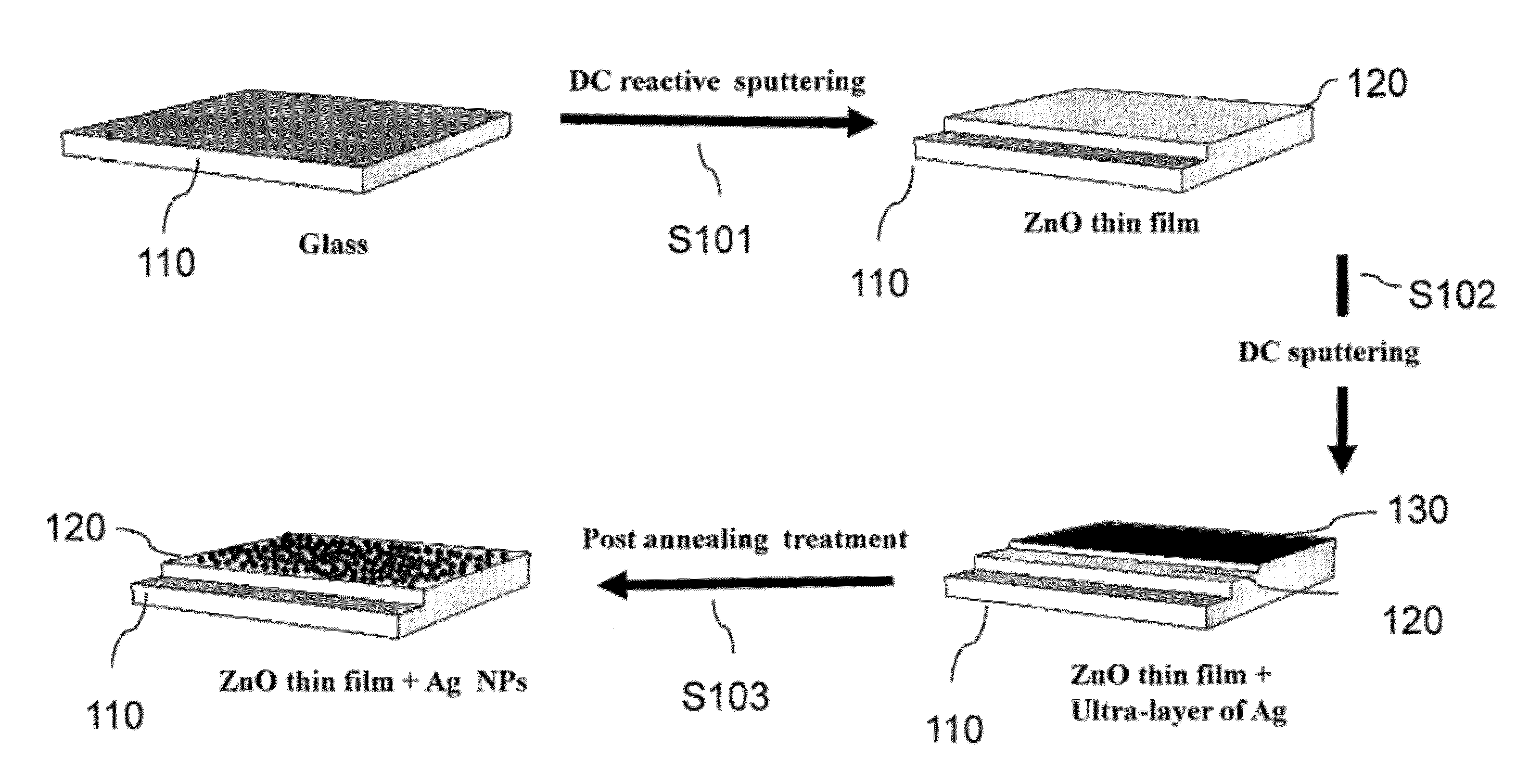
[0063]Thin layers of metallic silver were obtained by DC sputtering technique using an Automatic sputter coater (model NSC-4000).
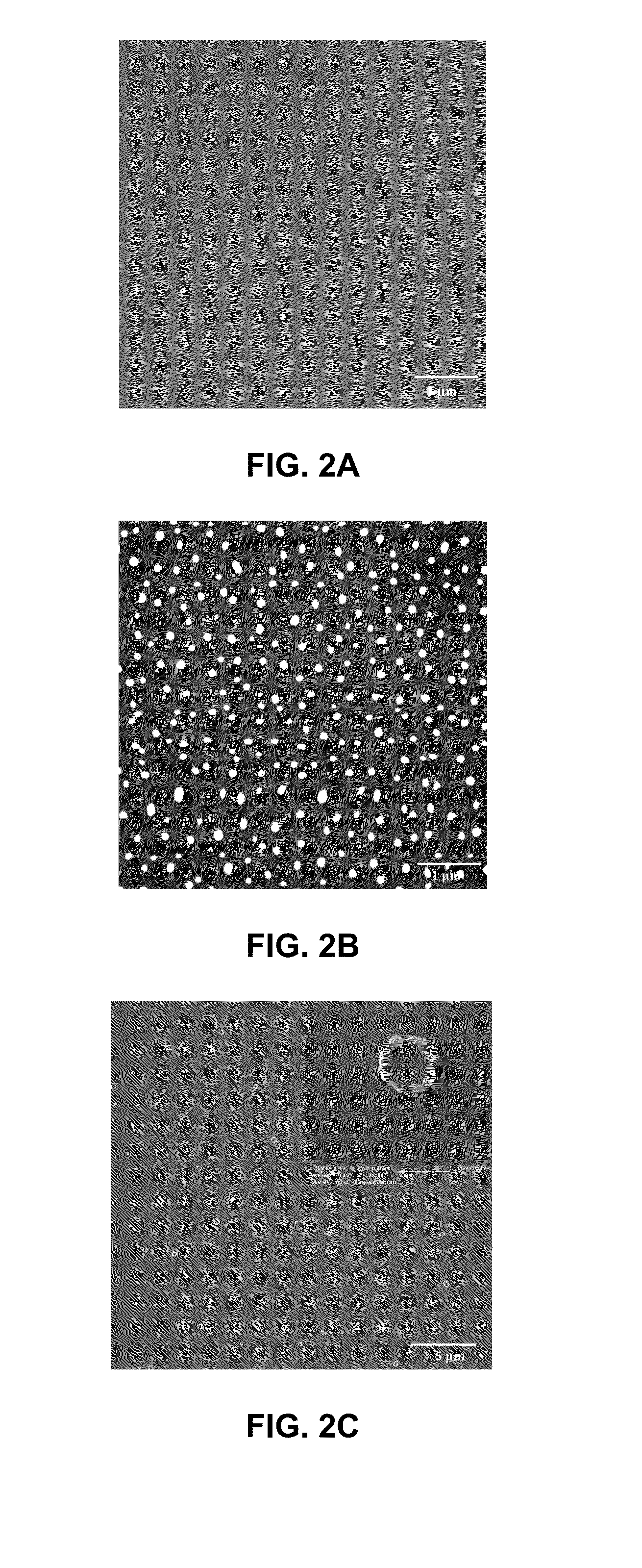
[0064]Referring to FIG. 1, wherein a Ag-NP synthesis process 100 is depicted. At step S101, a ZnO thin film 120 was deposited onto a glass substrate 110 using reactive plasma of pure oxygen (O2) and pure zinc target (99.999%). The deposition time was 25 minutes at 100 watt. FIG. 2A shows an SEM image of the ZnO thin film 120 formed at step S101.
[0065]At step S102, Ag was sputtered under pure Ar plasma using a pure silver target (99.99%) to form an Ag thin film 130 layered on top of the ZnO thin film 120. The deposition time ranged from 5 s to 25 s.
[0066]Before sputtering, the glass substrate 100 was cleaned using ethanol. The pure Zn and Ag targets were ultrasonicated for 15 min in acetone followed by 15 min ultrasonic cleaning in methanol.
[0067]Both steps S101 (sputtering of Zn) and S102 (sputtering of Ag) were carried out in a sputteri...
example 2
X-Ray Photoelectron Spectroscopy (XPS) Analysis
[0069]After step S102, wherein Ag was deposited on the ZnO thin film 120 by DC sputtering, the Ag / ZnO thin film 130 product was examined and analyzed for purity with an XPS spectroscope (ESCALAB 250Xi).
[0070]FIGS. 3A-3C show a wide scan spectrum, a high resolution Ag3d XPS spectrum and Zn2p spectra of the Ag / ZnO thin film 130 formed at step S102, respectively. The wide scan spectrum of FIG. 3A reflected the presence of Zn, O, Ag and C and no other contaminations were detected on the sample. The Ag3d XPS spectrum of FIG. 3B was fitted using two peaks, with the major peak centered at 367.8 eV being associated with metallic silver and the second peak at 368.9 eV probably associated with silver oxide (Ag2O). As shown in FIG. 3C, the positions of the Zn2p3 / 2 peak and 2p1 / 2 peak of the Ag / ZnO thin film 130 are 1021.18 eV and 1044.28 eV respectively, and they correspond to the peak positions of pure ZnO in the primary Zn2p XPS region.
example 3
Morphological Studies of Ag-NPs Annealed under Different Conditions
[0071]The Ag-NPs obtained from the synthesis process 100 were subject to morphological studies (particle size distribution, average particle size, density or average distance between particles, shape) using a Field emission scanning electron microscope (FESEM) (LYRA-3 Tescan).
[0072]FIGS. 4A-4D are FESEM images of Ag-NPs after annealing treatments at T=200° C., 400° C., 600° C. and 700° C. for 4 h under Ar atmosphere. As shown in FIG. 4A, a relatively smooth surface was observed after 200° C. treatment.
[0073]As shown in FIG. 4B, a very dense distribution of circular Ag-NPs was obtained after a 400° C. annealing treatment. The size distribution of the Ag-NPs was very broad, with the average particle size ranging from about 20 nm to 100 nm.
[0074]As seen in FIG. 4C, the annealing at 600° C. reduced the density of Ag-NPs to an average distance of 350 nm between particles. The size distribution was also narrowed to an aver...
PUM
| Property | Measurement | Unit |
|---|---|---|
| Temperature | aaaaa | aaaaa |
| Temperature | aaaaa | aaaaa |
| Time | aaaaa | aaaaa |
Abstract
Description
Claims
Application Information
 - R&D
- Intellectual Property
- Life Sciences
- Materials
- Tech Scout
- Unparalleled Data Quality
- Higher Quality Content
- 60% Fewer Hallucinations
Browse by: Latest US Patents, China's latest patents, Technical Efficacy Thesaurus, Application Domain, Technology Topic, Popular Technical Reports.
© 2025 PatSnap. All rights reserved.Legal|Privacy policy|Modern Slavery Act Transparency Statement|Sitemap|About US| Contact US: help@patsnap.com