
Automatic Defect Classification Without Sampling and Feature Selection

a technology of automatic defect classification and feature selection, applied in the field of automatic defect classification systems and methods, can solve the problems of large unclassified defect fraction, difficult to discover discriminating features, and the state of the art in automatic defect classification still requires operator intervention, so as to reduce the size and variation of the first feature map

Active Publication Date: 2016-06-09
KLA TENCOR TECH CORP
View PDF4 Cites 134 Cited by
  • Summary
  • Abstract
  • Description
  • Claims
  • Application Information

AI Technical Summary

Benefits of technology

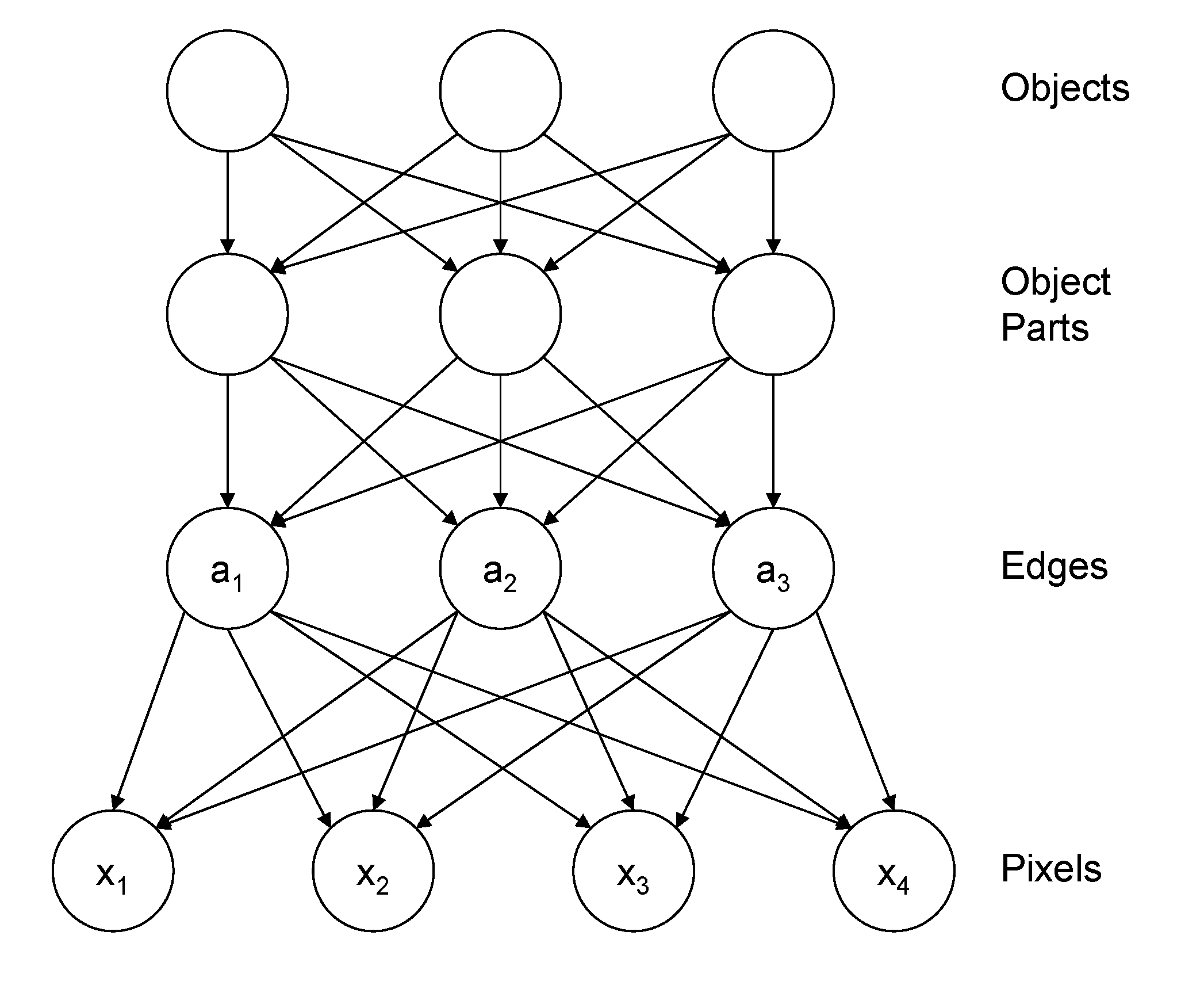
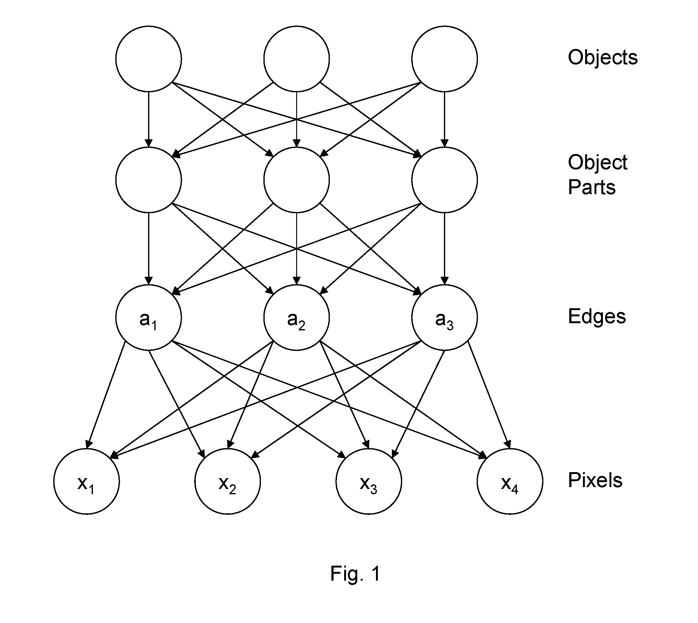
The present disclosure provides a system and method for defect classification in a semiconductor process using a deep-architecture neural network. The system extracts features from a defect image of a wafer and determines the classification of the defect based on the extracted features. The system includes a communication line for receiving the defect image, a deep-architecture neural network, and a classifier. The system can also include one or more convolution layers, subsampling layers, and a feature library for storing statistically significant features derived from defect images. The technical effects of the invention are improved efficiency and accuracy in defect classification, which can help improve the manufacturing process of semiconductor devices.

Problems solved by technology

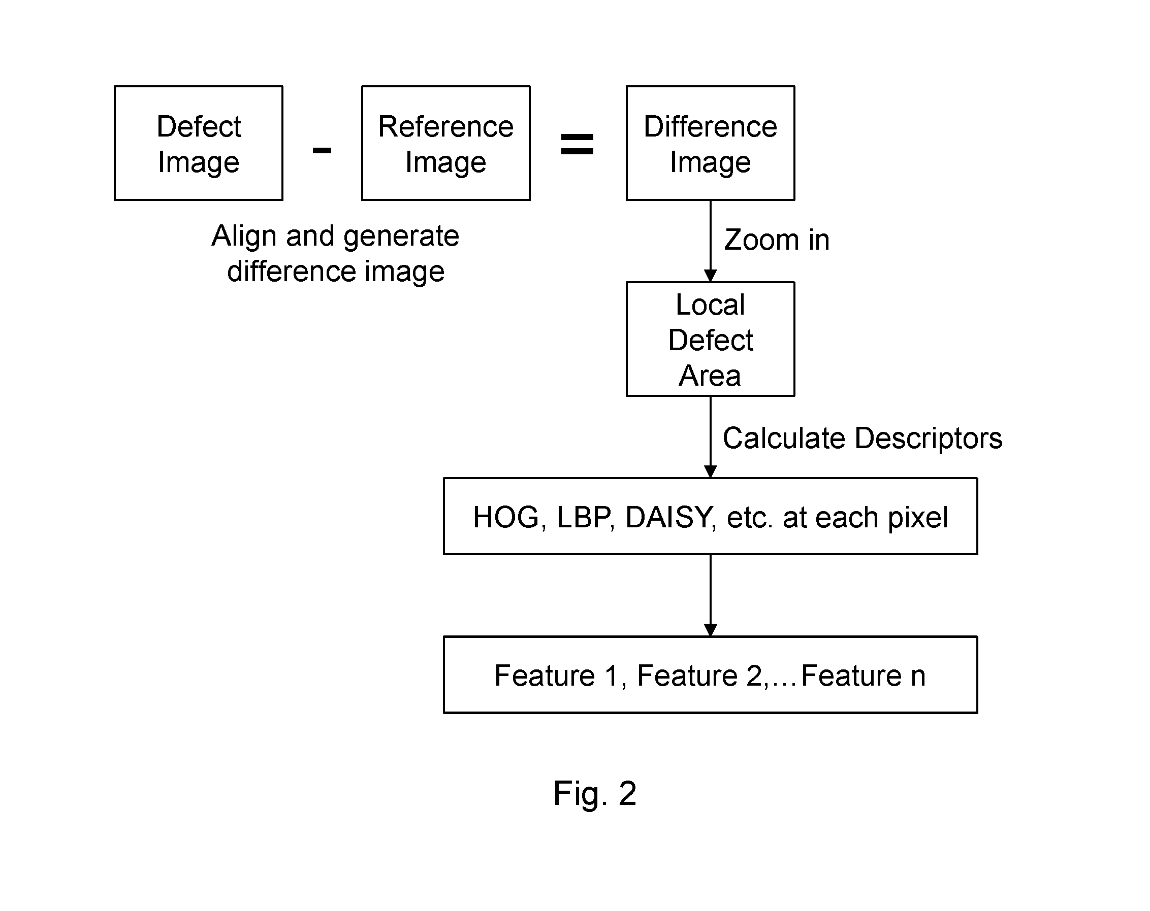
The current state of the art in automatic defect classification still requires operator intervention since typical automated techniques still leave a significant portion of defects unclassified.
Yet discriminating features are hard to discover and have are often maintained as secrets in many commercial defect review and classification systems.
It is well known that most image processing techniques focus on extracting low-level features, and that designing features for high-level object representation is very difficult.
In addition, features that can be used to classify one set of defect images may not work at all for other data sets.
Such inconsistent classification causes unnecessary confusion or even contradiction in the process control of wafer manufacturing.
One well-known issue with the above mentioned approaches is the contribution of classifier.
However, the throughput of defect review systems in production environments makes it impossible for operators to manually classify the remaining images.
With a 60%-70% automated classification rate, it still leaves ˜6,000-8,000 defects per hour that need to be manually classified by an operator.
However, these systems require a training phase in production and an expert defined feature set, which can impact the production ramp as well as require highly trained operator to identify the feature set.

Method used


Image

  • Automatic Defect Classification Without Sampling and Feature Selection
  • Automatic Defect Classification Without Sampling and Feature Selection
  • Automatic Defect Classification Without Sampling and Feature Selection

Examples


Embodiment Construction

[0025]The systems and methods of the present disclosure describe a new approach that eliminates the training / setup phase in automated defect classification (ADC) system. Although the new approach may require a large amount of defect images and time to build a machine-learning defect classification system, once the learning has been achieved and the library is in place, it can be leveraged to offset the impact incurred during set up. Often, many images are collected during the acceptance process before a tool is shipped to a customer. Such images can be utilized for the learning process. Once deployed, the new ADC approach can immediately generate defect class codes without any human intervention. The productivity impact is significant.

[0026]For example, using the presently disclosed system and method, there is no need for sampling and verification from operators, thereby saving manpower. No classifier setup process is required and ramp time improves. Inconsistencies and variations c...


PUM


Abstract

Systems and methods for defection classification in a semiconductor process are provided. The system includes a communication line configured to receive a defect image of a wafer from the semiconductor process and a deep-architecture neural network in electronic communication with the communication line. The neural network has a first convolution layer of neurons configured to convolve pixels from the defect image with a filter to generate a first feature map. The neural network also includes a first subsampling layer configured to reduce the size and variation of the first feature map. A classifier is provided for determining a defect classification based on the feature map. The system may include more than one convolution layers and / or subsampling layers. A method includes extracting one or more features from a defect image using a deep-architecture neural network, for example a convolutional neural network.

Description

CROSS-REFERENCE TO RELATED APPLICATIONS[0001]This application claims priority to the provisional patent application filed Dec. 3, 2014 and assigned U.S. App. No. 62 / 087,180 and to the provisional patent application filed Jun. 11, 2015 and assigned U.S. App. No. 62 / 174,288, the disclosures of which are hereby incorporated by reference.FIELD OF THE DISCLOSURE[0002]The disclosure relates to systems and methods for automatic defect classification in semiconductor manufacturing tools.BACKGROUND OF THE DISCLOSURE[0003]In manufacturing semiconductor devices, a defect review system is used to classify defects within a semiconductor process and can help in narrowing down the root cause of a defect or an excursion of the process. The defect review system does this by acquiring high resolution images around defect areas at a sub-micron level. Based on the acquired images, the system or an operator can classify the defects into categories in accordance with the type of the defects and how the d...

Claims


Application Information

Patent Timeline
IPC IPC(8): G06T7/00G06K9/62G06K9/66
CPCG06T7/0004G06T2207/30148G06K9/6255G06K9/66G06V10/454G06V2201/06G06F18/24143G06T2207/20081G06T2207/20084G06N3/084G06V30/19173G06N3/047G06N3/044G06N3/045G06V30/194G06F18/28
Inventor CHANG, WEIOLAVARRIA, RAMONRAO, KRISHNA
Owner KLA TENCOR TECH CORP
Learn More