Semiconductor device and display device

a display device and semiconductor technology, applied in semiconductor devices, instruments, computing, etc., can solve the problems of inability to accurately detect inputs, inability to reduce thickness, and inability to smoothly perform inputs, so as to improve the reliability of display modules, reduce thickness, and reduce inputs. uneven

Inactive Publication Date: 2016-06-02
SEMICON ENERGY LAB CO LTD
View PDF2 Cites 26 Cited by
  • Summary
  • Abstract
  • Description
  • Claims
  • Application Information

AI Technical Summary

Benefits of technology

[0010]In view of the above technical background, an object of one embodiment of the present invention is to provide a display module including a touch sensor in which wrong input can be reduced. Another object of one embodiment of the present invention is to improve the reliability of a display module including a touch sensor.
[0011]When a display module including a touch sensor is fabricated, a touch sensor overlaps with a display panel, which makes it difficult to reduce the thickness. An object of one embodiment of the present invention is to reduce the thickness of a display module including a touch sensor. Another object of one embodiment of the present invention is to reduce the weight of a display module including a touch sensor.
[0012]When a display module including a touch sensor is fabricated, a touch sensor and a display panel are fabricated separately and then need to be combined with each other, which leads to an increase in fabricating cost. An object of one embodiment of the present invention is to prevent an increase in fabricating cost of a display module including a touch sensor.

Problems solved by technology

Thus, some problems arise in that input is not smoothly performed, for example.
Specifically, when the display surface is seen diagonally through a touch sensor, icons displayed on the display surface deviate from the sensing positions of the touch panel, which inhibits an accurate input.
When a display module including a touch sensor is fabricated, a touch sensor overlaps with a display panel, which makes it difficult to reduce the thickness.
When a display module including a touch sensor is fabricated, a touch sensor and a display panel are fabricated separately and then need to be combined with each other, which leads to an increase in fabricating cost.

Method used


Image

  • Semiconductor device and display device
  • Semiconductor device and display device
  • Semiconductor device and display device

Examples


embodiment 1

[0051]In this embodiment, a touch sensor and a liquid crystal display device integrated with a touch sensor, of one embodiment of the present invention, are described (FIGS. 1A and 1B).

[0052]FIG. 1A illustrates a schematic view of a display device integrated with an active matrix touch sensor of one embodiment of the present invention. A display device 10 integrated with an active matrix touch sensor of one embodiment of the present invention includes a display region 100, a gate line 104 provided in the display region 100, a gate line driver circuit 20 electrically connected to the gate line 104, a source line 105 provided in the display region 100, a source line driver circuit 30 electrically connected to the source line 105, a bus line 102 provided in the display region 100, a sensor unit driver circuit 40 for the active matrix touch sensor electrically connected to the bus line 102, a bus line 103 provided in the display region 100, a conversion circuit 50 for the active matrix ...

embodiment 2

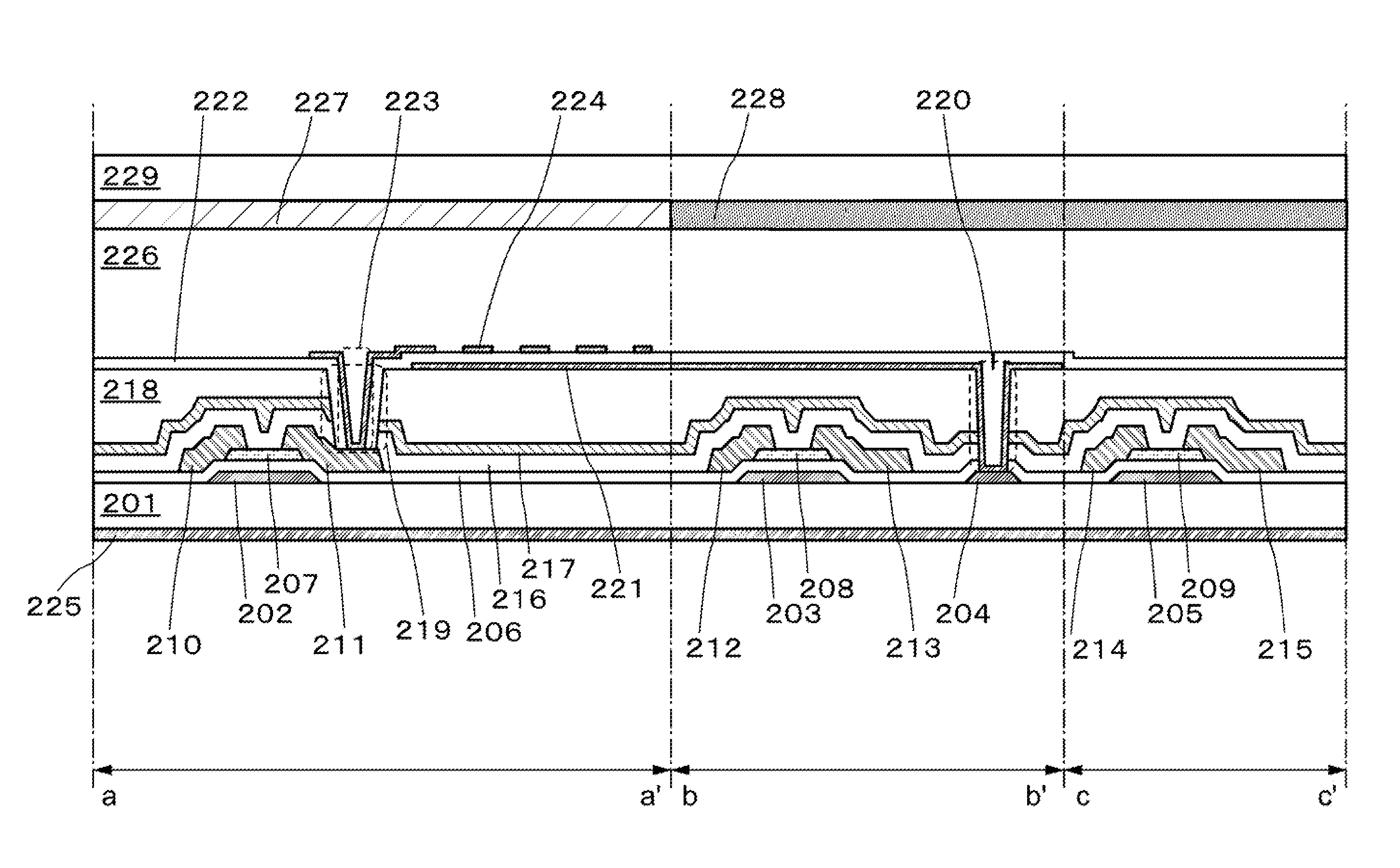
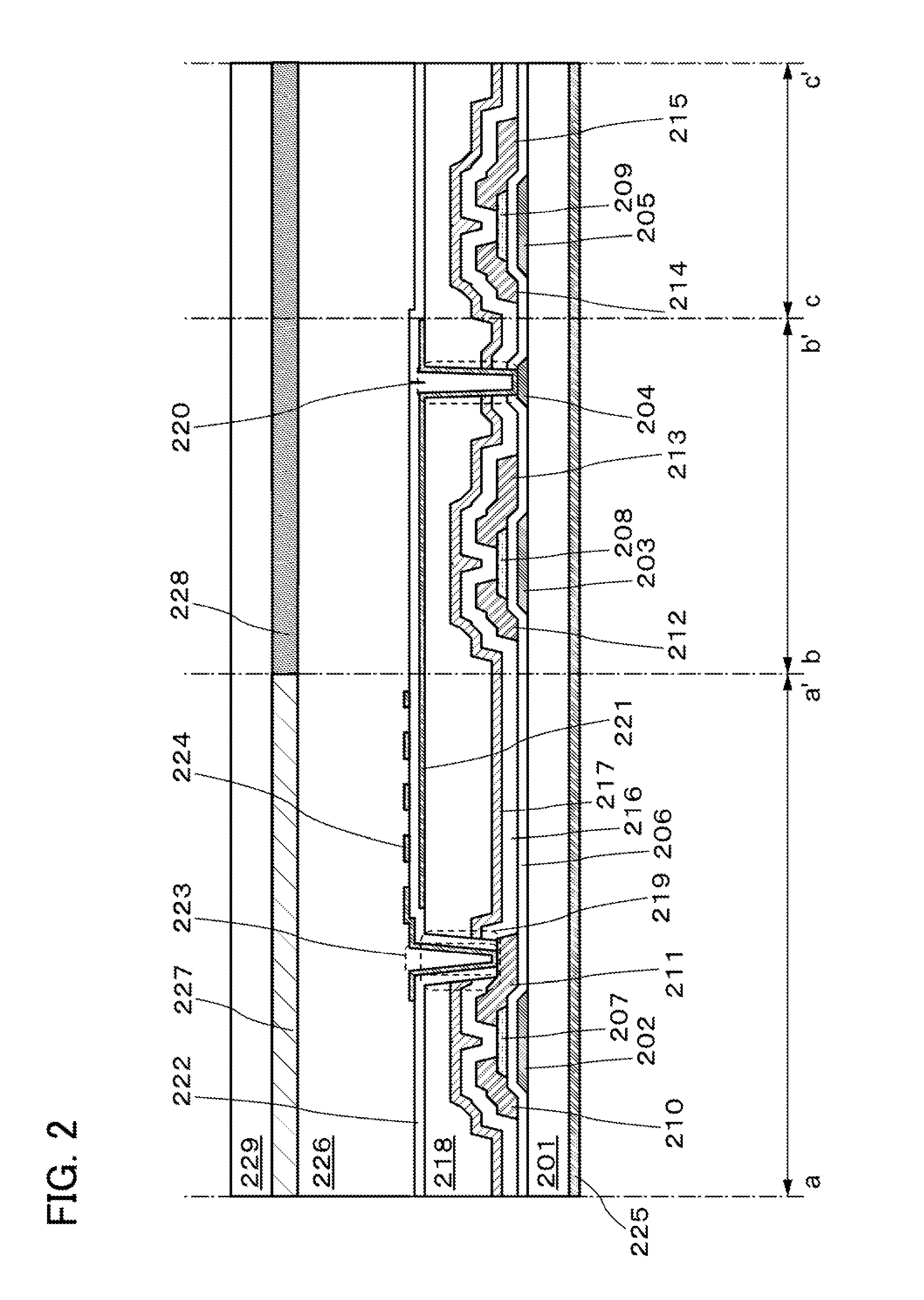
[0063]FIG. 3 is a cross-sectional view of a liquid crystal display device integrated with an active matrix touch sensor of one embodiment of the present invention. In FIG. 3, a cross section a-a′ illustrates part of a display element; b-b′, a sensor unit; and c-c′, part of circuit.

[0064]FIG. 2 illustrates a structure in which the conductive film 225 is provided under the substrate 201. FIG. 3 illustrates an example in which a conductive film 301 corresponding to the conductive film 225 is provided on the substrate 229 side. Since the structure provided over the substrate 201 in FIG. 3 is similar to that of FIG. 2 except for the conductive film 225, the description is omitted. An example in which a conductive film 301 is provided over the liquid crystal is described in FIG. 3.

[0065]In one embodiment of the present invention, the conductive film 301 overlaps with the conductive film 224 with the liquid crystal layer 226 interposed therebetween. In the structure of FIG. 3, the liquid c...

embodiment 3

[0068]In this embodiment, a driving method by which the frequency of screen updating is reduced as much as possible is described as a method for driving a liquid crystal of one embodiment of the present invention.

[0069]A liquid crystal display device to which the driving method is applied displays images by at least two driving methods (modes). One is a driving method in which screen updating is successively performed. This method is called “normal driving.” The other is a driving method in which screen writing is stopped after screen writing processing is executed. This method is called “idling stop (IDS) driving. In a “normal mode (state)” and an “IDS mode (state),” the liquid crystal display device is operated by the normal drive and the IDS drive, respectively.

[0070]Moving images are displayed by the normal drive. Still images are displayed by the normal drive or the IDS drive. For displaying still images, the same picture is displayed; therefore, screen updating is not necessar...


PUM

PropertyMeasurementUnit
specific resistivityaaaaaaaaaa
frame frequencyaaaaaaaaaa

Abstract

An increase in fabricating cost of a display module including a touch sensor is suppressed. A display device which includes a first substrate, a second substrate, and liquid crystal interposed between the first substrate and the second substrate includes a display portion. The display portion includes a sensor unit and a pixel. The sensor unit includes a first transistor, a first conductive film electrically connected to a gate of the first transistor, and a second conductive film. At least part of the first conductive film overlaps with at least part of the second conductive film. The pixel includes a second transistor, and a pixel electrode electrically connected to the second transistor. At least part of the pixel electrode overlaps with at least part of the first conductive film.

Description

BACKGROUND OF THE INVENTION[0001]1. Field of the Invention[0002]One embodiment of the present invention relates to a touch sensor. Another embodiment of the present invention relates to a display device including a touch sensor or a display panel, or a touch sensor and a display panel in combination.[0003]Note that the term “display panel” in this specification and the like means all display devices such as a liquid crystal panel, an organic EL panel, and an inorganic EL panel. The term “semiconductor device” means all devices which can operate by utilizing semiconductor characteristics. A semiconductor element such as a transistor, a semiconductor circuit, an arithmetic device, and a memory device are each an embodiment of a semiconductor device. An imaging device, a display device, a liquid crystal display device, a light-emitting device, an electro-optical device, and an electronic device may have a semiconductor device. In addition, a display device including a touch sensor and ...

Claims


Application Information

Patent Timeline
Patent Type & Authority Applications(United States)
IPC IPC(8): G02F1/1333G02F1/1343H01L29/24G02F1/1368H01L27/12H01L29/786
CPCG02F1/13338H01L27/1225H01L29/7869H01L29/24G02F1/1368G02F1/134309G02F1/13454H01L27/1255G06F3/0412
Inventor HATSUMI, RYOISHITANI, TETSUJI
Owner SEMICON ENERGY LAB CO LTD
Why Eureka
Try Eureka