Chip antenna for near field communication and method of manufacturing the same

a near field communication and chip technology, applied in the direction of antennas, antenna details, antenna feed intermediates, etc., can solve the problems of reducing radiation efficiency and gain of on-chip antennas, limiting the bandwidth of the whole system, and reducing the radiation efficiency of on-chip antennas. the effect of reducing power loss and maximizing bandwidth

Active Publication Date: 2016-04-28
SAMSUNG ELECTRONICS CO LTD +1
View PDF7 Cites 2 Cited by
  • Summary
  • Abstract
  • Description
  • Claims
  • Application Information

AI Technical Summary

Benefits of technology

[0010]One or more exemplary embodiments are chip antennas for near field communication that maximize bandwidth and antenna efficiency by reducing power loss and may be used for miniaturization.

Problems solved by technology

Also, in this process, even though the antenna itself has a broadband characteristic, a bandwidth limitation may occur in the whole system.
Therefore, by taking into account the cost for separately manufacturing the antenna and the additional cost for connecting the chip to the antenna, the off-chip antenna is not suitable for communicating between chips.
However, power loss due to the high resistance and high dielectric constant of silicon, radiation efficiency and gain of the on-chip antenna may be reduced.
In the case of a general dipole antenna, it is difficult to apply the general dipole antenna to a system that requires a broadband characteristic due to the narrow band width of the general dipole antenna.
Also, the exemplary embodiments are not required to overcome the disadvantages described above, and may not overcome any of the problems described above.

Method used


Image

  • Chip antenna for near field communication and method of manufacturing the same
  • Chip antenna for near field communication and method of manufacturing the same
  • Chip antenna for near field communication and method of manufacturing the same

Examples


Embodiment Construction

[0037]Exemplary embodiments are described in greater detail below with reference to the accompanying drawings.

[0038]In the following description, like drawing reference numerals are used for like elements, even in different drawings. The matters defined in the description, such as detailed construction and elements, are provided to assist in a comprehensive understanding of the exemplary embodiments. However, it is apparent that the exemplary embodiments can be practiced without those specifically defined matters. Also, well-known functions or constructions are not described in detail since they would obscure the description with unnecessary detail.

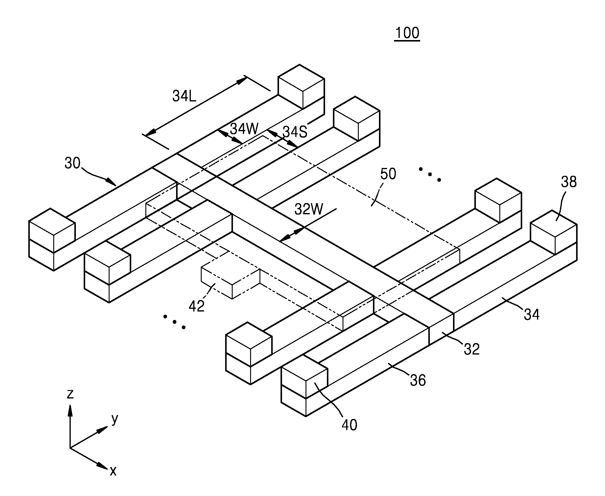
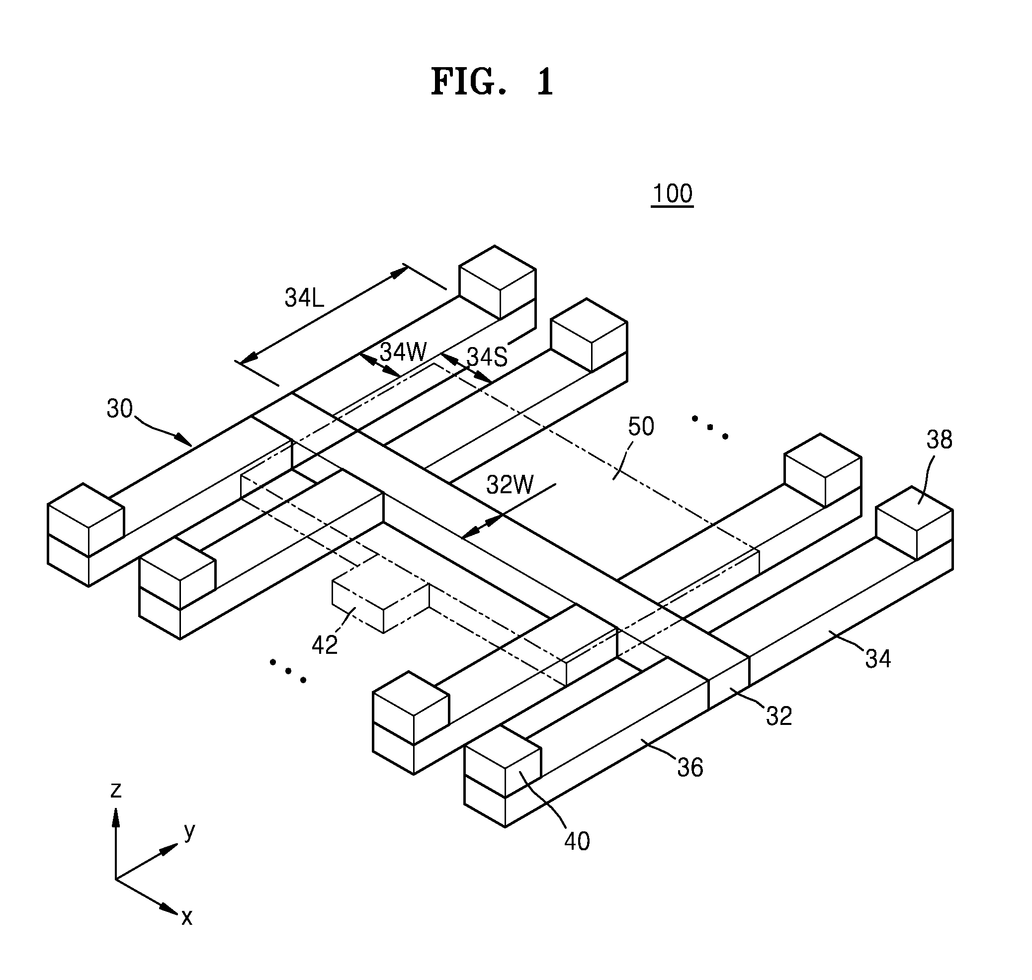
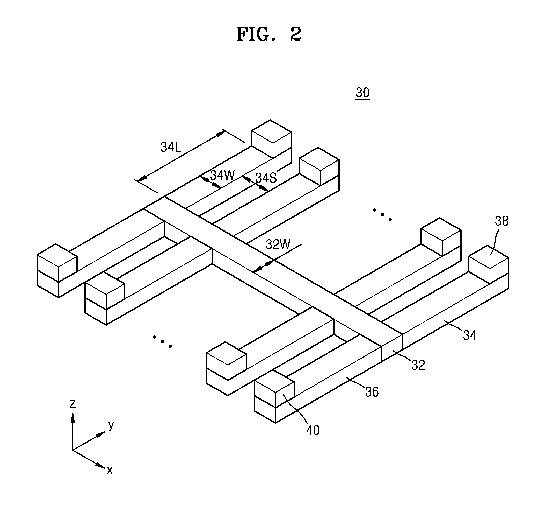
[0039]FIG. 1 is a perspective view of a chip antenna 100 for near field communication (hereinafter, referred to as ‘a chip antenna 100’) according to an exemplary embodiment.

[0040]Referring to FIG. 1, the chip antenna 100 includes a first antenna element 30 and a second antenna element 50. The second antenna element 50 may be formed on th...


PUM


Abstract

Provided are chip antennas for near field communication and methods of manufacturing the chip antennas. A chip antenna for near field communication includes a substrate; a first antenna element on the substrate; and a second antenna element on the first antenna element. The substrate, the first antenna element, and the second antenna element are included in a single chip. The first and second antenna elements are formed outside the chip. The substrate is a lower layer including a plurality of devices. The first antenna element is a metal structure having a fish bone shape. The second antenna element is a dipole antenna.

Description

CROSS-REFERENCE TO RELATED APPLICATION[0001]This application claims priority from Korean Patent Application No. 10-2014-0144286, filed on Oct. 23, 2014 in the Korean Intellectual Property Office, the disclosure of which is incorporated herein in its entirety by reference.BACKGROUND[0002]1. Field[0003]Apparatuses and methods consistent with exemplary embodiments relate to communication devices, and more particularly, to chip antennas for near field communication and methods of manufacturing the chip antennas.[0004]2. Description of the Related Art[0005]An antenna is one of the elements that constitute a radio frequency (RF) wireless communication system. Radiation efficiency and gain of the antenna may be important factors for evaluating the power efficiency of the RF wireless communication system. If radiation efficiency and gain of the antenna are high, a burden of a power amplifier that consumes large power may be reduced in an RF wireless communication system and power efficiency...

Claims


Application Information

Patent Timeline
Patent Type & Authority Applications(United States)
IPC IPC(8): H01Q9/28
CPCH01Q9/28H01Q1/2283
Inventor PARK, CHULSOONKIM, HOJUNGKIM, HONGYIOH, INNYEALLEE, JOONGHOJANG, TAEHWAN
Owner SAMSUNG ELECTRONICS CO LTD
Why Eureka
Try Eureka