Scheme to measure individually rise and fall delays of non-inverting logic cells

Active Publication Date: 2016-03-03
STMICROELECTRONICS INT NV
View PDF2 Cites 1 Cited by
  • Summary
  • Abstract
  • Description
  • Claims
  • Application Information

AI Technical Summary

Benefits of technology

The logic cell delay test and characterization circuit can accurately measure both the rising edge and falling edge delays of a logic cell. This is achieved by measuring the duration of an oscillator circuit in two modes: a first mode where the signal is propagated through the logic cells and a second mode where the signal is propagated through a smaller subset of logic cells. By dividing the difference in periods by the number of logic cells, the precise delay of the signal through a single logic cell can be calculated. This circuit provides a reliable and accurate tool for testing and characterizing the performance of logic circuits.

Problems solved by technology

Likewise, if the output of the OR gate is high, after the OR gate receives low signals on all of its inputs there is some delay before the output of the OR gate goes low.
In other words, there is a first kind of delay when the rising edge of the signal is received at the inputs of the logic cell.
There is a second kind of delay when a falling edge of the logic signal is received at the inputs of the logic signal.
Prior ring oscillator methods for measuring the delay of logic cells have only provided an average of both the rise and fall delay of the logic cells.

Method used


Image

  • Scheme to measure individually rise and fall delays of non-inverting logic cells
  • Scheme to measure individually rise and fall delays of non-inverting logic cells
  • Scheme to measure individually rise and fall delays of non-inverting logic cells

Examples


Embodiment Construction

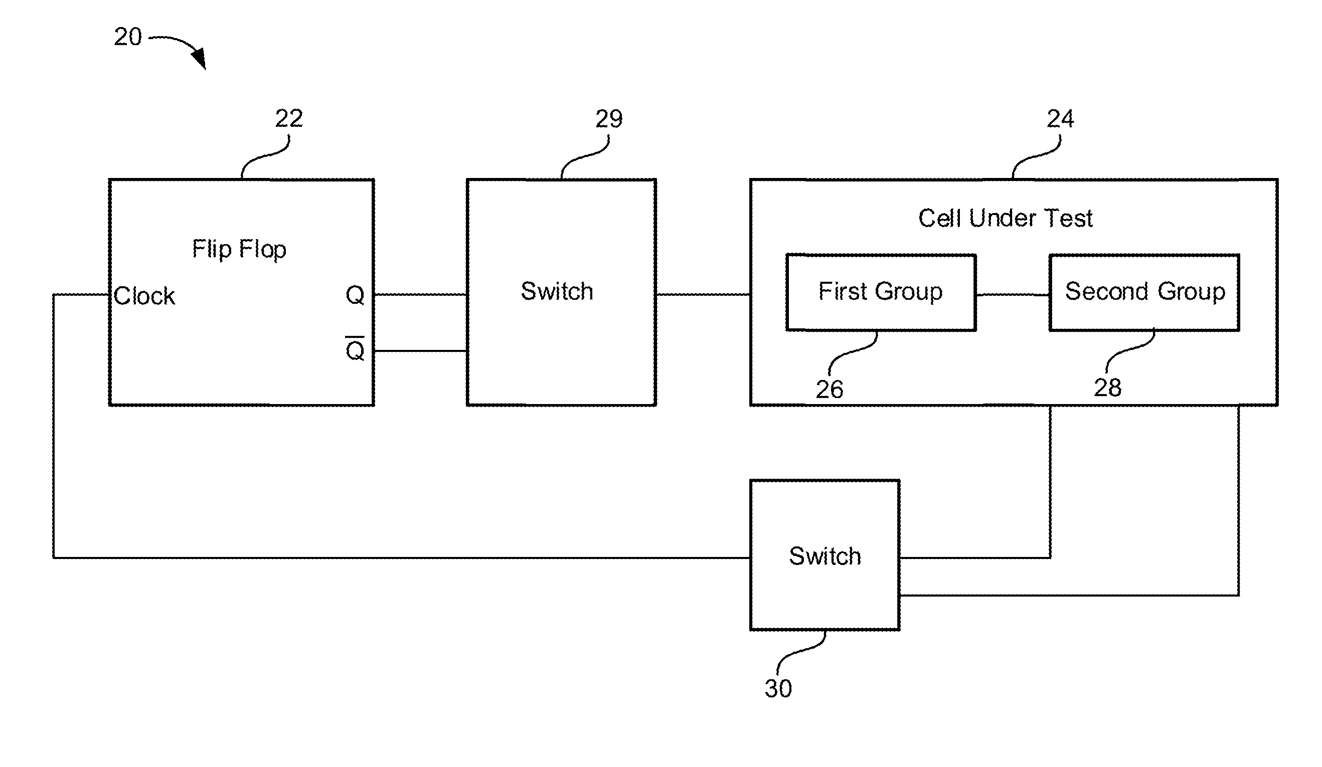
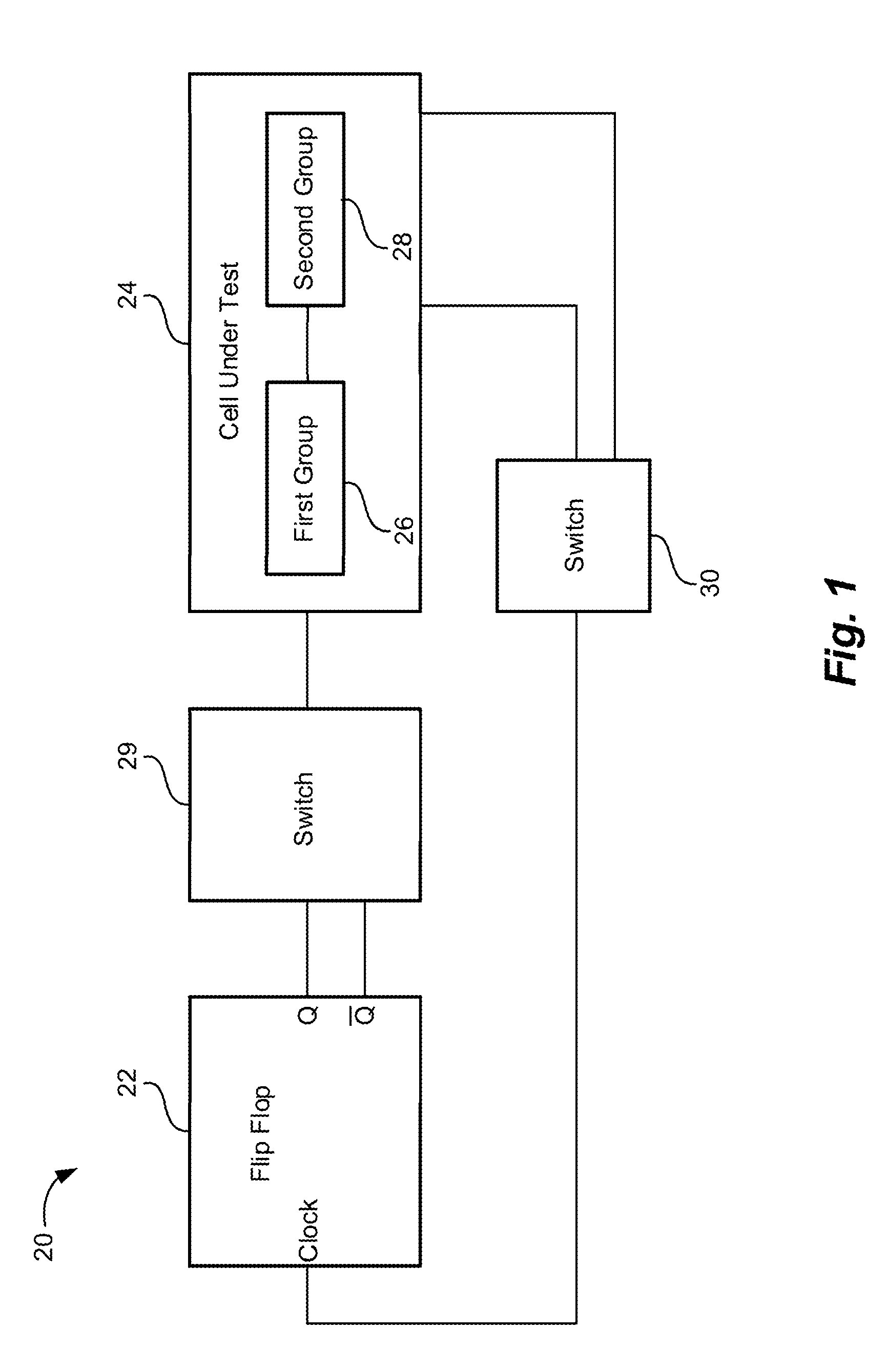
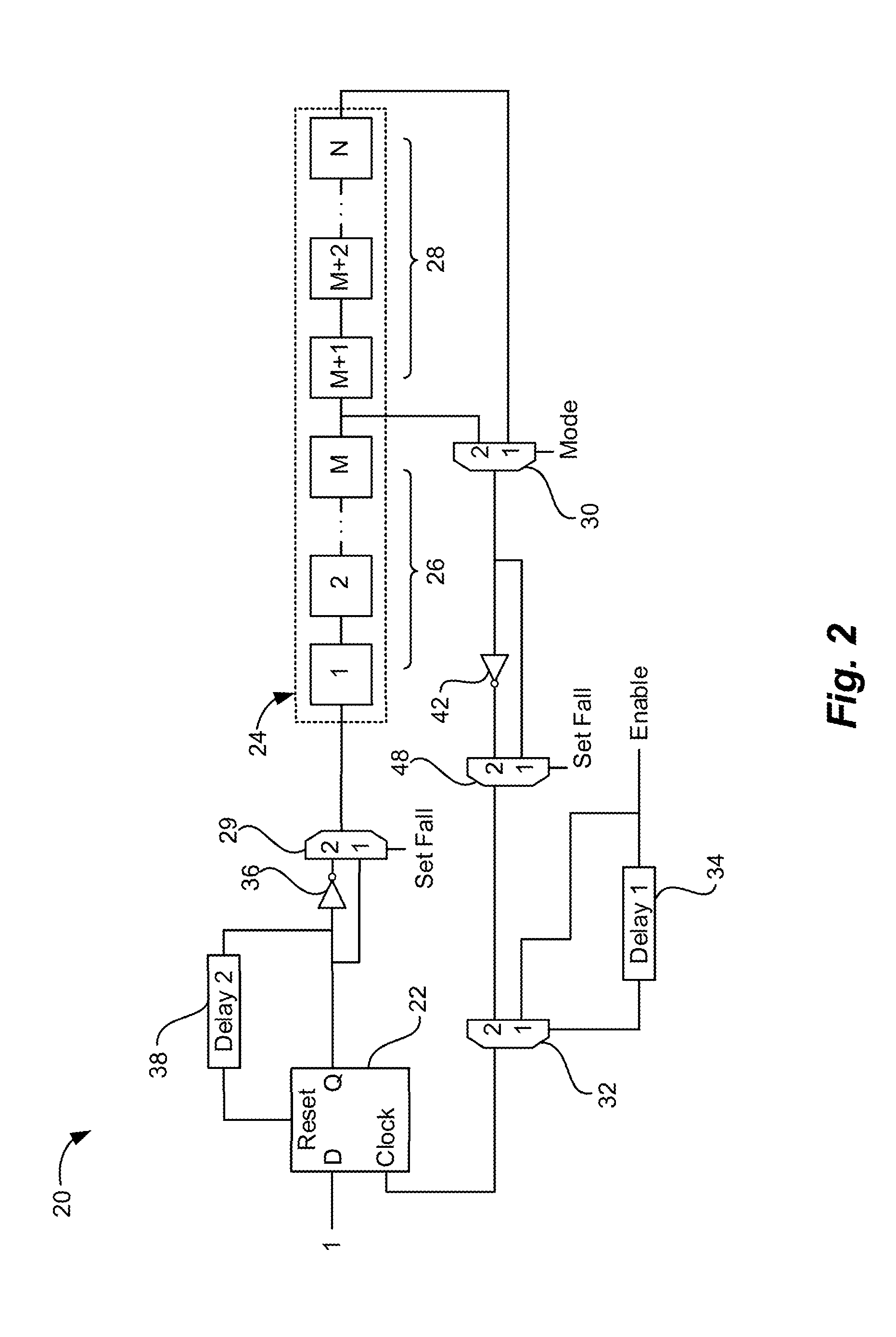
[0023]FIG. 1 is a block diagram of a logic cell delay test and characterization circuit according to one embodiment. The logic cell delay test and characterization circuit 20 includes a flip-flop 22, a chain of logic cells 24 including a first group 26 of logic cells and a second group 28 of logic cells coupled to the flip-flop 22 in a ring oscillator configuration. A first switch 29 is coupled between the output of the flip-flop 22 and the input of the cells under test 24. A second switch 30 is coupled between the output of the cells under test 24 and the input of the flip-flop 22.

[0024]The test and characterization circuit 20 of FIG. 1 makes advantageous use of a property of flip-flop type ring oscillators in which the frequency of flip-flop ring oscillators depends only on one type of signal transition, either the rising edge signal transition or the falling edge signal transition. The test and characterization circuit 20 uses the chain of logic cells under test 24 as a delay ele...


PUM


Abstract

A test circuit measures both the rising edge delay and the falling edge delay associated with a logic cell. The test circuit includes a flip-flop type ring oscillator with two groups of logic cells connected in series in the oscillation path. A first multiplexor switches the ring oscillator between a rising edge and a falling edge mode. A second multiplexer causes the second group of logic cells to be included or excluded from the oscillation path. By measuring the oscillation period in the various modes, the rising edge and falling edge delays can be individually calculated.

Description

BACKGROUND[0001]1. Technical Field[0002]The present disclosure relates to the field of testing and characterization of signal propagation delay of logic cells. The present disclosure relates more particularly to the field of testing and characterization of the propagation delay of both rising edge signals and falling edge signals in logic cells.[0003]2. Description of the Related Art[0004]Digital integrated circuits typically include many different kinds of logic cells. Types of logic cells include OR gates, AND gates, NOR gates, NAND gates, inverters, buffers, and many other kinds of logic cells. Digital integrated circuits can include millions or even billions of transistors connected together in a complex organization to form the various circuits of the digital integrated circuit.[0005]Logic cells commonly receive a signal on one or more inputs and output a signal in accordance with the inputs. For each kind of logic cell there is some delay from the time it takes after receiving...

Claims


Application Information

Patent Timeline
IPC IPC(8): G01R31/317G01R31/3177
CPCG01R31/3177G01R31/31725
Inventor SINGH, SAURABH, KUMARSINGH, BALWANT
Owner STMICROELECTRONICS INT NV
Why Eureka
Try Eureka