Data processing device
a data processing and data technology, applied in the field of data processing devices, can solve the problems of increasing overhead and increasing power consumption, and achieve the effect of reducing power consumption
- Summary
- Abstract
- Description
- Claims
- Application Information
AI Technical Summary
Benefits of technology
Problems solved by technology
Method used
Image

Examples
first embodiment
Instruction Cache Common Bus
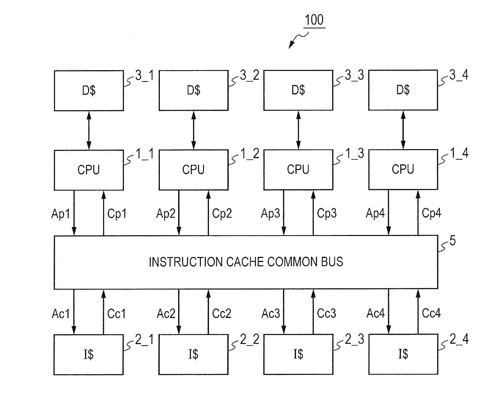
[0101]FIG. 1 is a block diagram showing a configuration example of a data processing device according to the first embodiment.
[0102]The data processing device 100 according to the first embodiment includes CPUs 1_1 to 1_4, instruction cache memories (I$) 2_1 to 2_4 and data cache memories (D$) 3_1 to 3_4 corresponding to the CPUs 1_1 to 1_4, and includes an instruction cache common bus 5 between the CPUs 1_1 to 1_4 and the instruction cache memories 2_1 to 2_4. These components are coupled via multibit digital signal interconnections, but bus notation is omitted in FIG. 1. The same applies to the other drawings in the present application.
[0103]The CPUs 1_1 to 1_4 issue addresses Ap1 to Ap4 for instruction fetch to the instruction cache common bus 5, respectively.
[0104]When the parallel-operating CPUs 1_1 to 1_4 operate independently in the MIMD type, the addresses Ap1 to Ap4 issued at the same time generally do not assume the same value, because the CPUs ...
second embodiment
Common Bus (Switching and Coexistence of Bus Arbitration / Broadcast)
[0131]FIG. 6 is a block diagram showing a configuration example of a data processing device 100 according to the second embodiment.
[0132]In the data processing device 100 according to the second embodiment, the four CPUs 1_1 to 1_4 are coupled to a memory 7 through a common bus 6. The four CPUs 1_1 to 1_4 output the addresses Ap1 to Ap4 for instruction fetch, thereby to make requests to the common bus 6 for bus rights. In the common bus 6, a bus arbitration circuit (not shown) performs arbitration based on predetermined priorities. In order in which the CPUs acquire the bus right, an address Am is issued to the memory 7, and an instruction code Cm is read and fetch. When some or all of the four CPUs 1_1 to 1_4 operate parallelly in the SIMD type, in the second embodiment, the common bus 6 makes only one access to an address requested by the CPUs operating in the SIMD type, and parallelly supplies (broadcasts) the rea...
third embodiment
Parallel Cache Fill by Broadcast
[0144]FIG. 9 is a block diagram showing a configuration example of a data processing device 100 according to the third embodiment.
[0145]The data processing device 100 according to the third embodiment includes the CPUs 1_1 to 1_4, the instruction cache memories (I$) 2_1 to 2_4 and the data cache memories (D$) 3_1 to 3_4 corresponding to the CPUs 1_1 to 1_4, the common bus 6, and the main memory 7.
[0146]The CPUs 1_1 to 1_4 issue addresses Ap1 to Ap4 for instruction fetch to the corresponding instruction cache memories 2_1 to 2_4 respectively, and the instruction cache memories 2_1 to 2_4 supply instruction codes Cp1 to Cp4 for operation. When a cache miss occurs in any of the instruction cache memories 2_1 to 2_4, the corresponding cache fill address Af1 to Af4 is issued to the common bus 6, and access to the main memory 7 is requested. The main memory 7 is accessed, with the address of the access request that has acquired a bus right by bus arbitratio...
PUM
 Abstract
Description
Claims
Application Information
 - R&D
- Intellectual Property
- Life Sciences
- Materials
- Tech Scout
- Unparalleled Data Quality
- Higher Quality Content
- 60% Fewer Hallucinations
Browse by: Latest US Patents, China's latest patents, Technical Efficacy Thesaurus, Application Domain, Technology Topic, Popular Technical Reports.
© 2025 PatSnap. All rights reserved.Legal|Privacy policy|Modern Slavery Act Transparency Statement|Sitemap|About US| Contact US: help@patsnap.com