
Ultra low silicon loss high dose implant strip

a high-dose, ultra-low silicon technology, applied in the direction of photomechanical treatment, instruments, electrical equipment, etc., can solve the problems of oxidation of implant atoms in resists, sputtering during high-energy implants, and removing some of the underlying functional device structure, etc., to achieve the effect of low silicon loss

Active Publication Date: 2015-11-19
NOVELLUS SYSTEMS
View PDF6 Cites 3 Cited by
  • Summary
  • Abstract
  • Description
  • Claims
  • Application Information

AI Technical Summary

Benefits of technology

This approach achieves a substantially residue-free strip process with low silicon loss, compatible with metal gates and suitable for high-dose ion implantation, improving the yield and reducing the need for additional residue removal processing steps.

Problems solved by technology

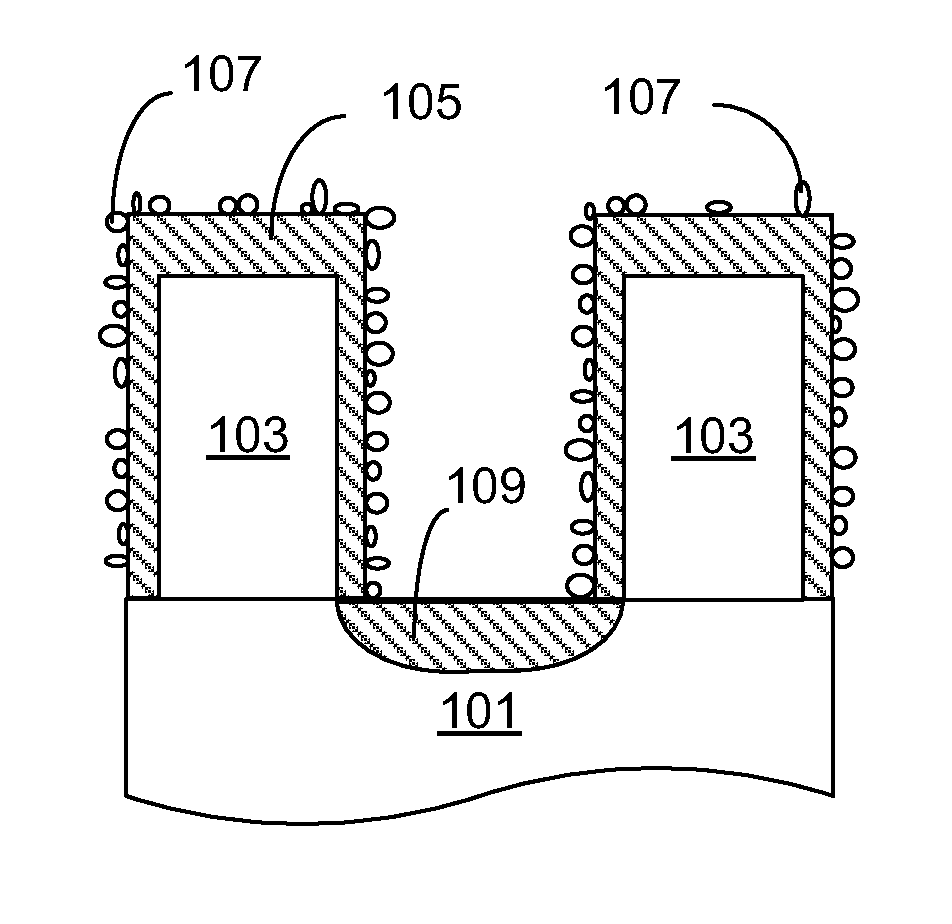
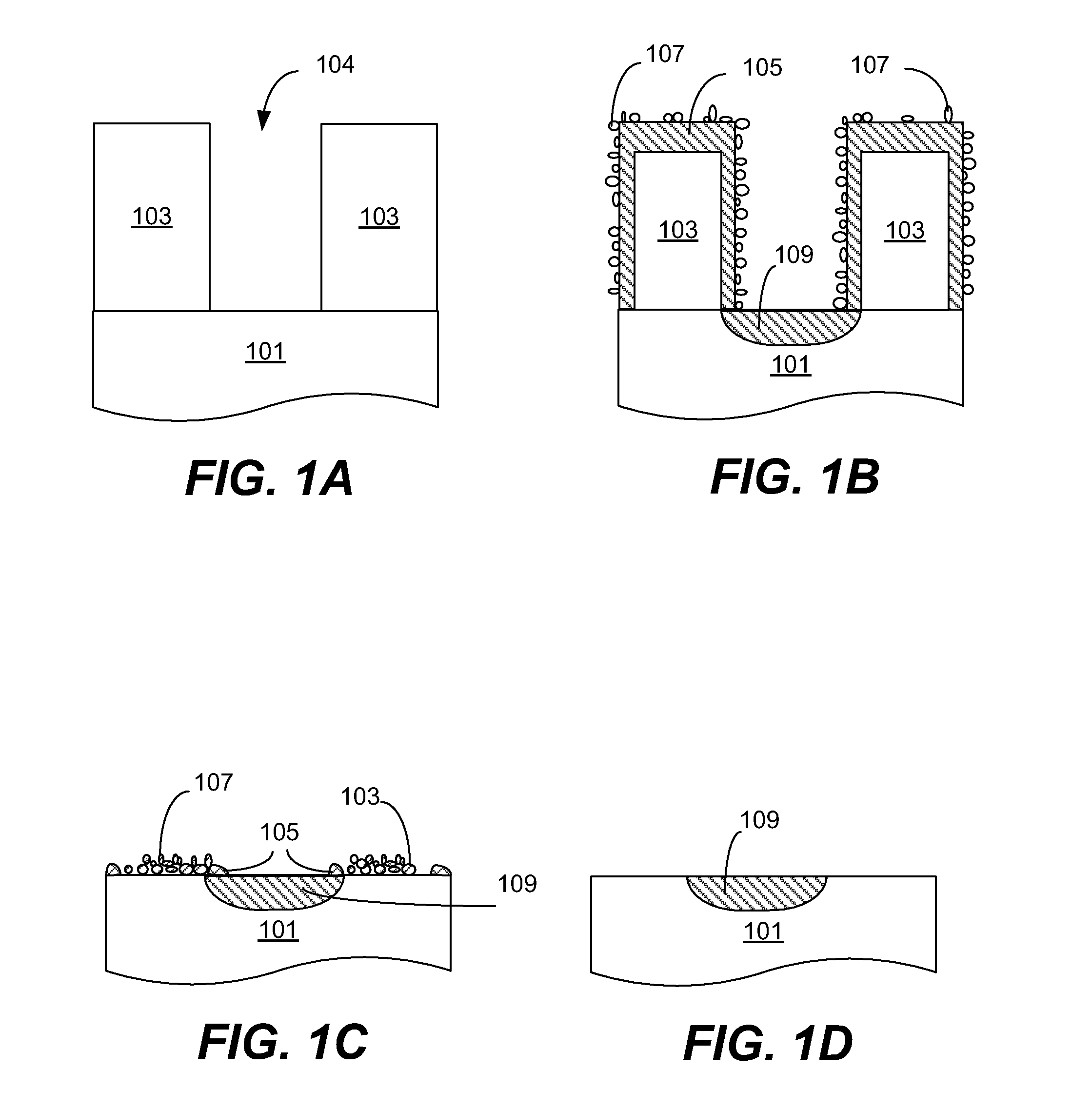
They may result from sputtering during the high-energy implant, incomplete removal of crust, and / or oxidation of implant atoms in the resist.
Unfortunately, in conventional HDIS operations, overstripping sometimes removes some of the underlying functional device structure.
At the device layer, even very little silicon loss from the transistor source / drain regions may adversely affect device performance and yield, especially for ultra shallow junction devices fabricated at the <32 nm design rule or below.

Method used


Image

  • Ultra low silicon loss high dose implant strip
  • Ultra low silicon loss high dose implant strip
  • Ultra low silicon loss high dose implant strip

Examples


example processes

[0070]As indicated above, in certain embodiments, a multi-station strip apparatus is employed to perform the photoresist and residue stripping processes described herein. FIG. 7 is a simplified schematic showing a top view of such an apparatus including stations 1, 2, 3, 4, 5 and 6. Wafers enter the apparatus at station 1 via chamber 701, are transferred to each station in sequence for a processing operation at that station and exit from station 6 via chamber 702 after the process is complete. The architecture allows hydrogen based residue free high dose implant strip process with low silicon loss and TiN metal gate compatibility.

example process 1

[0071]

H2CO2NF3CF4FlowFlowFlowFlowTemper-RateRateRateRateatureStationOperation(lpm)(sccm)(sccm)(sccm)(C.)1Pre-heat00002402Crust Removal2-332151002403-5Bulk2-33215100285PhotoresistStrip6Overash and2-332500350Residue Clean

[0072]The above process is an example of a process sequence including a NF3 spike in station 6.

example process 2

[0073]

H2CO2NF3CF4FlowFlowFlowFlowTemper-RateRateRateRateatureStationOperation(lpm)(sccm)(sccm)(sccm)(C.)1Pre-heat00002402Crust Removal2-33215100240(2-Stage)501003-5Bulk2-33215100285PhotoresistStrip6Overash and2-332500350Residue Clean

[0074]The above process is an example of a process sequence including a NF3 spike for half of the exposure time in station 2, during crust removal. For example, a wafer may be in the station for 18 seconds, with NF3 spiked for the second 9 seconds.


PUM


Abstract

Improved methods for stripping photoresist and removing ion implant related residues from a work piece surface are provided. According to various embodiments, plasma is generated using elemental hydrogen, a fluorine-containing gas and a protectant gas. The plasma-activated gases reacts with the high-dose implant resist, removing both the crust and bulk resist layers, while simultaneously protecting exposed portions of the work piece surface. The work piece surface is substantially residue free with low silicon loss.

Description

CROSS-REFERENCE TO RELATED APPLICATIONS[0001]This application is a continuation of and claims priority to U.S. patent application Ser. No. 12 / 636,582, titled “ULTRA LOW SILICON LOSS HIGH DOSE IMPLANT STRIP”, filed Dec. 11, 2009, which is hereby incorporated by reference in its entirety and for all purposes.FIELD OF INVENTION[0002]The present invention pertains to methods and apparatuses to remove or strip photoresist material and removing related residues from a work piece surface. In certain embodiments, this application relates to methods and apparatus for stripping resist after ion implant or plasma assisting doping implant (low dose or high-dose implanted resist).BACKGROUND[0003]Photoresist is a light sensitive material used in certain fabrication processes to form a patterned coating on a work piece, e.g., a semiconductor wafer, during processing. After exposing the photoresist coated surface to a pattern of high energy radiation, a portion of the photoresist is removed to reve...

Claims


Application Information

Patent Timeline
Patent Type & Authority Applications(United States)
IPC IPC(8): H01L21/311
CPCH01L21/31138G03F7/427H01L21/3065H01L21/31116H01L21/31144H01L21/32136H01L21/32137H01L21/32139
Inventor CHEUNG, DAVIDFANG, HAOQUANKUO, JACKKALINOVSKI, ILIALI, ZHAOYAO, ANDREWGUHA, ANIRBANOSTROWSKI, KIRK
Owner NOVELLUS SYSTEMS
Learn More