Capacitive sensing array device with high sensitivity and high frame rate and electronic apparatus using the same

a sensing array and high frame rate technology, applied in the direction of resistance/reactance/impedence, instruments, pulse techniques, etc., can solve the problems of large sensing error, high cost, and decrease in sensitivity, and achieve high frame rate, high sensitivity, and high sensitivity

Inactive Publication Date: 2015-08-20
J METRICS TECH CO LTD
View PDF3 Cites 18 Cited by
  • Summary
  • Abstract
  • Description
  • Claims
  • Application Information

AI Technical Summary

Benefits of technology

[0013]It is therefore an object of the invention to provide a capacitive sensing array device with a high sensitivity and a high frame rate, and an electronic apparatus usin

Problems solved by technology

However, the too-thick protection layer causes the very small sensing capacitance, thereby decreasing the sensitivity.
So, the cost is high.
If the thickness control of the package substrate, the thickness control of the chip and the like are considered at the same time, this distance further causes the great sensing error.
Consequently, in addition to the high cost, it is a g

Method used


Image

  • Capacitive sensing array device with high sensitivity and high frame rate and electronic apparatus using the same
  • Capacitive sensing array device with high sensitivity and high frame rate and electronic apparatus using the same
  • Capacitive sensing array device with high sensitivity and high frame rate and electronic apparatus using the same

Examples


Embodiment Construction

[0029]The present invention will be apparent from the following detailed description, which proceeds with reference to the accompanying drawings, wherein the same references relate to the same elements.

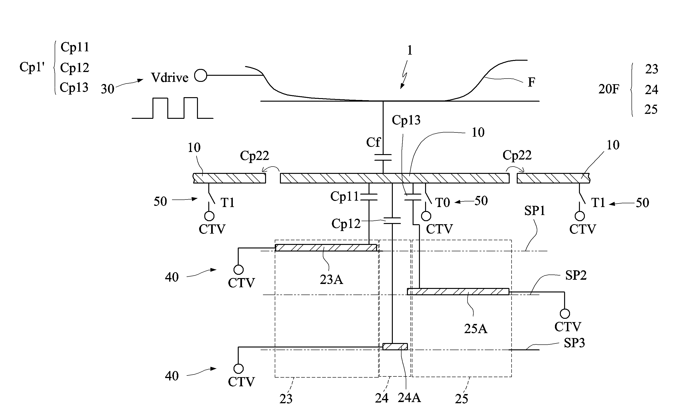
[0030]FIG. 3 is a schematic illustration showing a structure of a capacitive sensing array device 1 according to a first embodiment of the invention. FIG. 4 is a schematic illustration partially showing a structure design of sensing electrodes of the capacitive sensing array device 1 according to the first embodiment of the invention. FIG. 5 is a schematic illustration showing a single sensing member and its corresponding sensing circuit of the capacitive sensing array device 1 according to the first embodiment of the invention. Referring to FIGS. 3 to 5, the capacitive sensing array device 1 of this embodiment includes sensing electrodes 10, a shielding conductor layer 20, a coupling signal source 30, a constant voltage source 40, switch modules 50, a semiconductor substrate 65, a pa...


PUM


Abstract

In a capacitive sensing array device and an electronic apparatus, a coupling signal source provides a coupling signal to an object, a constant voltage source provides a constant voltage to a shielding conductor group, and a vertical parasitic capacitor is formed between the shielding conductor group and each sensing electrode. Each sensing electrode is electrically connected to the constant voltage source via one corresponding switch module. When one sensing electrode is selected to perform sensing, the corresponding switch module is set as an open state such that the selected sensing electrode is disconnected from the constant voltage source, while the other sensing electrodes are electrically connected to the constant voltage source via their corresponding switch modules configured as short-circuit states, so that a horizontal parasitic capacitor is formed between the selected sensing electrode and the other sensing electrodes. The shielding conductor group comprises shielding conductor layers on shielding planes.

Description

[0001]This application is a Continuation-in-Part of co-pending application Ser. No. 14 / 045,514, filed on Oct. 3, 2013, and claims priority of No. 103116185 filed in Taiwan R.O.C. on May 7, 2014 under 35 USC 119, the entire content of which is hereby incorporated by reference.BACKGROUND OF THE INVENTION[0002]1. Field of the Invention[0003]The invention relates to a capacitive sensing array device and an electronic apparatus using the same, and more particularly to a capacitive sensing array device with a high sensitivity and a high frame rate, and an electronic apparatus using the same.[0004]2. Related Art[0005]The conventional capacitive sensing technology for sensing the skin of the human body may be applied to, for example, the fingerprint sensor for sensing finger's textures or a capacitive touch panel or a capacitive touch screen.[0006]More particularly, the basic structure of the portion of the sensor in contact with the skin's texture to sense the skin's texture is an array-ty...

Claims


Application Information

Patent Timeline
IPC IPC(8): G01R27/26G06F3/041G06F3/044
CPCG01R27/2605G06F2203/04107G06F3/0416G06F3/044H03K17/9622H03K2217/960705G06F3/04166G06F3/0443H01L2224/48091H01L2924/00014
Inventor CHOU, BRUCE C.S.
Owner J METRICS TECH CO LTD
Why Eureka
Try Eureka