
Circuit for Symbol Timing Synchronization

a timing synchronization and symbol technology, applied in the direction of transmission, modulated carrier system, automatic control of pulses, etc., can solve the problems of lack of flexibility to operate on different modulation schemes, near-optimum sampling instants,

Active Publication Date: 2015-08-06
STICHTING IMEC NEDERLAND
View PDF4 Cites 19 Cited by
  • Summary
  • Abstract
  • Description
  • Claims
  • Application Information

AI Technical Summary

Benefits of technology

The proposed solution allows for easy use with different standards by analyzing phase differences in digital data. It can detect timing errors and adjust the sampling instants accordingly. The timing synchronization circuit described in the patent offers the benefits of both acquisition and tracking.

Problems solved by technology

A general problem of timing synchronization in wireless systems is to find near-optimum sampling instants of baseband signals.
Many proposed solutions are tailored to a particular modulation scheme / wireless standard and lack the flexibility to operate on different modulation schemes.
Conventional solutions, however, are tailored to a particular modulation scheme or a wireless standard and lack flexibility to operate on different modulation schemes.
Furthermore, they are typically only used for timing acquisition in the preamble section of the wireless data packet, while for timing tracking another circuit is required as the data payload is unknown.
In addition they contain high complexity modules such as correlators, interpolators and decimation filters, and the like.
This increases the computational as well as the circuit complexity, and may lead to higher power consumption and larger silicon area.
However, correlation-based approaches are typically only employed for initial timing acquisition, not for timing tracking during frame reception, because of the higher costs in terms of power consumption (needs to be continuously active during the whole frame).
As already mentioned, several problems can be identified concerning current solutions for baseband symbol timing synchronization.
Current approaches offer limited flexibility (e.g., single standard support), hence a multitude of timing synchronization circuits is required to support different wireless standards.
Another problem relates to the high complexity of the applied timing synchronization algorithms.
Further, different circuits are needed for performing initial timing synchronization and timing tracking, which additionally contributes to higher complexity, higher power and area consumption.
The sharp phase transitions result in relatively prominent side-lobe levels of the signal spectrum compared to the main lobe, which means the signal should be transmitted in a wider frequency band, otherwise it ends up with increased interference levels in the adjacent channels.
Therefore, the receiver cannot make decisions on any isolated symbol without taking the previous symbols into account.
When the signal is low-pass filtered (as is typical in a transmitter), these phase shifts result in large amplitude fluctuations.
However, the drawback is that the Gaussian filter increases the modulation memory in the system and causes inter-symbol interference.
Therefore, in low power design, non-coherent suboptimal receivers are typically used to demodulate GFSK signals.
The proposed solution involves a high computational complexity and is vulnerable to frequency offset.
This approach, however, is limited to a specific baseband modulation scheme and / or symbol rate, i.e. DQPSK.
Furthermore, the output of the differential detector, and hence, the subsequent timing error detector is affected by the input signal amplitude.
Another limitation is that the carrier frequency offset compensation is applied to the signal after the timing error estimation.
Furthermore, the proposed solution directly modifies the sampling process of the ADC in the analog domain, which adds complexity to the ADC design and leads to phase distortion and slower timing loop settling time of the timing compensation.

Method used


Image

  • Circuit for Symbol Timing Synchronization
  • Circuit for Symbol Timing Synchronization
  • Circuit for Symbol Timing Synchronization

Examples


Embodiment Construction

[0050]The present disclosure will be described with respect to particular embodiments and with reference to certain drawings but the disclosure is not limited thereto but only by the claims.

[0051]Furthermore, the terms first, second and the like in the description and in the claims, are used for distinguishing between similar elements and not necessarily for describing a sequence, either temporally, spatially, in ranking or in any other manner. It is to be understood that the terms so used are interchangeable under appropriate circumstances and that the embodiments of the disclosure described herein are capable of operation in other sequences than described or illustrated herein.

[0052]It is to be noticed that the term “comprising”, used in the claims, should not be interpreted as being restricted to the means listed thereafter; it does not exclude other elements or steps. It is thus to be interpreted as specifying the presence of the stated features, integers, steps or components as...


PUM


Abstract

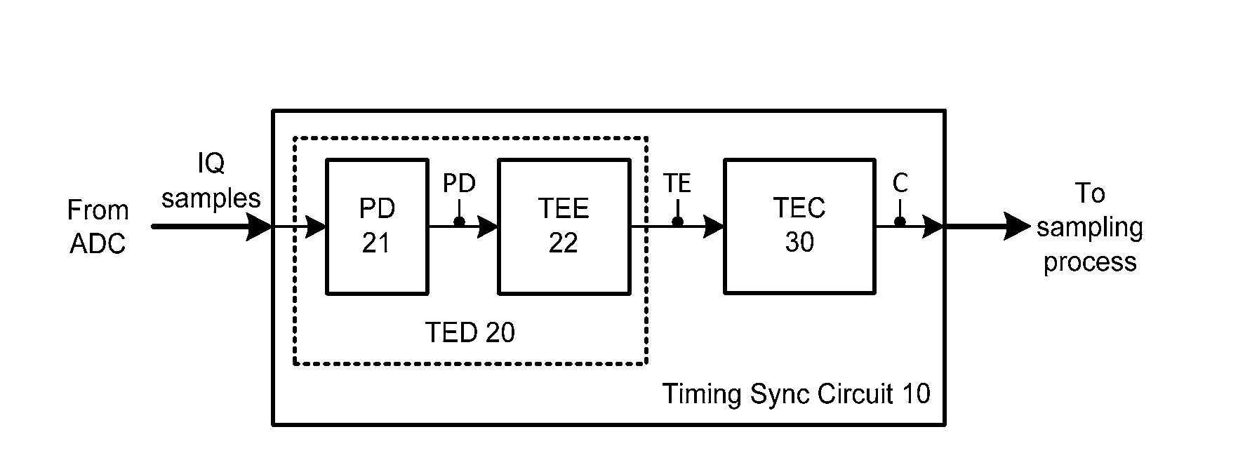
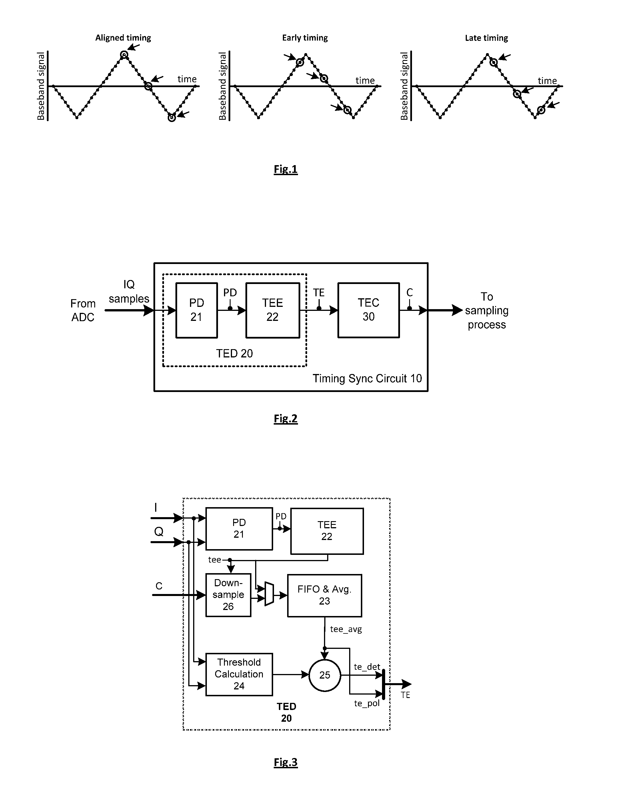
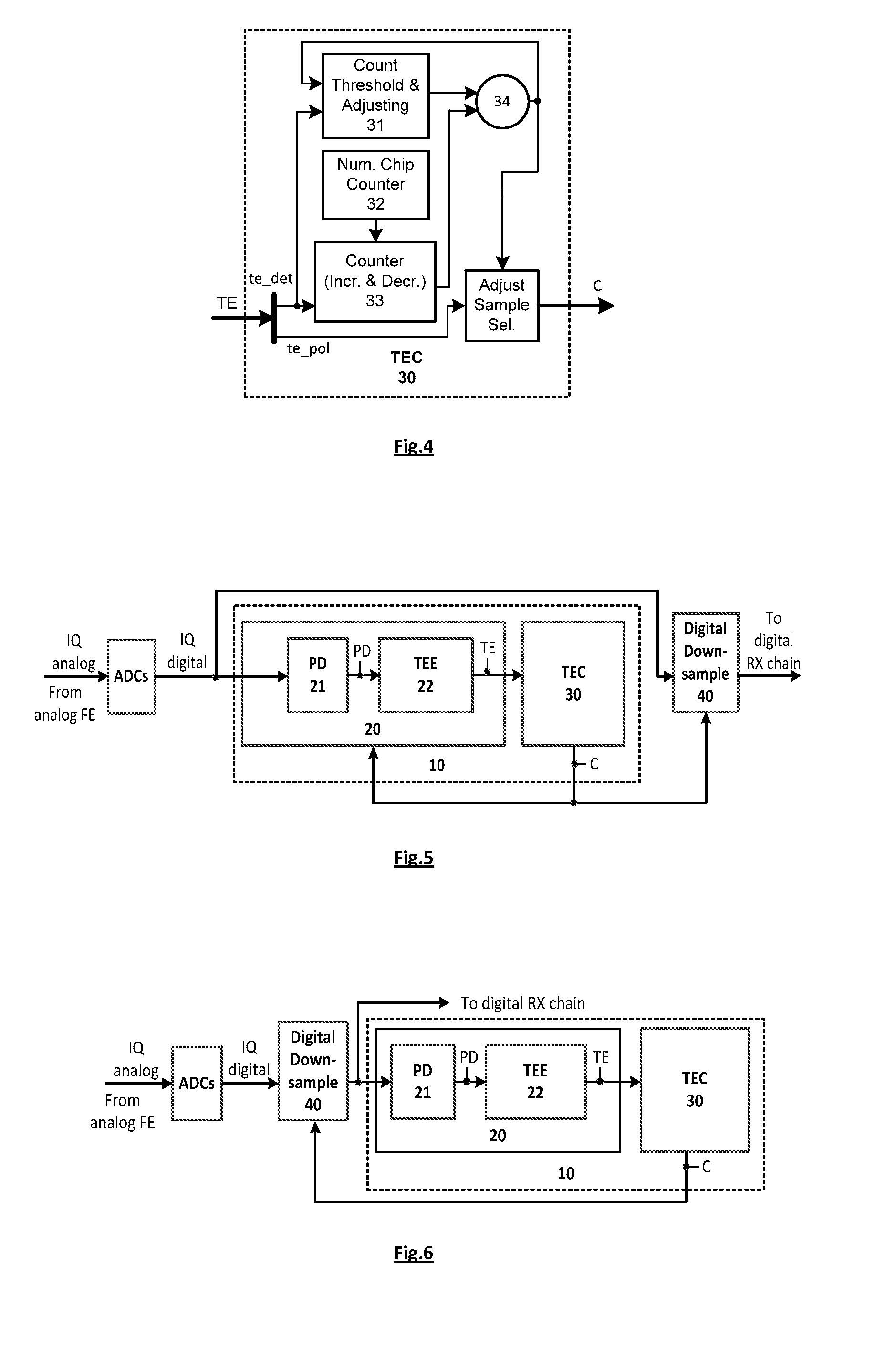
The present disclosure relates to a timing synchronization circuit for a digital receiver structure that includes a timing error detection module comprising a phase difference calculation unit arranged for calculating a phase difference between incoming samples of a digital data stream, and a timing error estimator arranged for determining a timing error estimate based on the calculated phase difference, and for generating, based on the determined timing error estimate, a signal indicative of timing error detection. The circuit also includes a timing error control module arranged for receiving the signal indicative of timing error detection, for evaluating the number of received signals indicative of timing error detection and for outputting, after comparison with a threshold value, a sampling adjustment command for adjusting the sampling instants applied for obtaining the digital data stream.

Description

CROSS-REFERENCE TO RELATED APPLICATION[0001]This application claims priority to European Patent Application No. 14153485.9 filed on Jan. 31, 2014, the contents of which are hereby incorporated by referenceTECHNICAL FIELD[0002]The present disclosure is generally related to the field of timing synchronization circuits.BACKGROUND[0003]Ultra-low-power (ULP) short-range wireless connectivity is becoming increasingly relevant to a wide range of sensor and actuator node applications ranging from consumer life style to medical applications. In recent years a multitude of wireless standards has been proposed to meet differing requirements of individual application domains such as data rates, range, Quality-of-Service (QoS), and peak and average power consumption. From a commercial perspective, a single radio component supporting multiple wireless standards—targeting at multiple application domains / markets—while reducing integration costs is preferable. In particular for mobile applications, ...

Claims


Application Information

Patent Timeline
Patent Type & Authority Applications(United States)
IPC IPC(8): H04L7/00H03L7/08
CPCH04L7/0054H03L7/08H04L7/0041H04L7/0087H04L7/0335H04L27/156H04L27/3854H04L7/0029H04L27/2331H04L7/0062H04L7/033H04L7/0008H04L7/0331H04L7/02H04L7/0004H04L7/007H03L7/091
Inventor BACHMANN, CHRISTIANZHANG, YAN
Owner STICHTING IMEC NEDERLAND
Learn More