Pattern Failure Discovery by Leveraging Nominal Characteristics of Alternating Failure Modes

a technology of alternating failure mode and failure mode, applied in the field of pattern failure discovery, can solve the problems of modulated dies, increased noise level, and inability to effectively sample defects, and achieve the effects of improving the noise level

Active Publication Date: 2015-07-16
KLA TENCOR TECH CORP
View PDF8 Cites 13 Cited by
  • Summary
  • Abstract
  • Description
  • Claims
  • Application Information

AI Technical Summary

Benefits of technology

[0021]FIG. 9 is a block diagram illustrating one embodiment of a non-transitory computer-readable medium that includes progra...

Problems solved by technology

However, as the dimensions of semiconductor devices decrease, inspection becomes even more important to the successful manufacture of acceptable semiconductor devices because smaller defects can cause the devices to fail.
The methods described above that use modulated dies have several challenges.
For example, too many defects can be detected in the methods described above, which impairs the ability to effectively sample defects.
In particular, when comparing highly modulated dies to a nominal die, detection is easier but at modulations near normal, the noise level can increase.
This results in a substantially high defect count and often makes it difficult to sample real defects.
Often, defect review time is wasted, and a defect review tool user may experience fatigue in looking at so many non-relevant patterns.
In other words, much effort can be wasted in inspecting and/or reviewing at irrelevant lithograp...

Method used


Image

  • Pattern Failure Discovery by Leveraging Nominal Characteristics of Alternating Failure Modes
  • Pattern Failure Discovery by Leveraging Nominal Characteristics of Alternating Failure Modes
  • Pattern Failure Discovery by Leveraging Nominal Characteristics of Alternating Failure Modes

Examples


Embodiment Construction

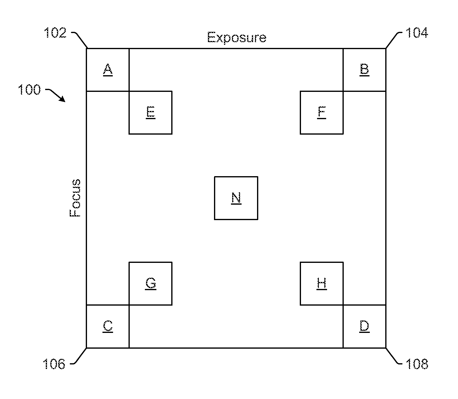
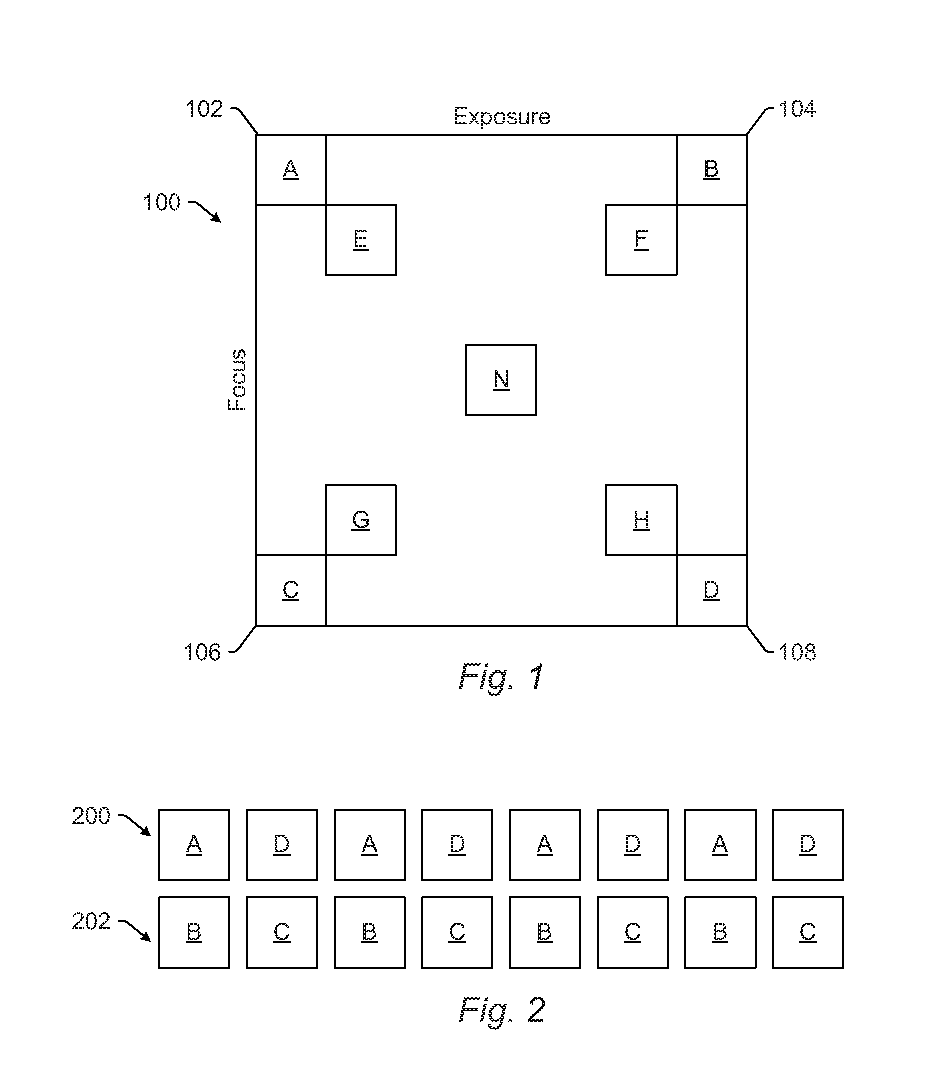
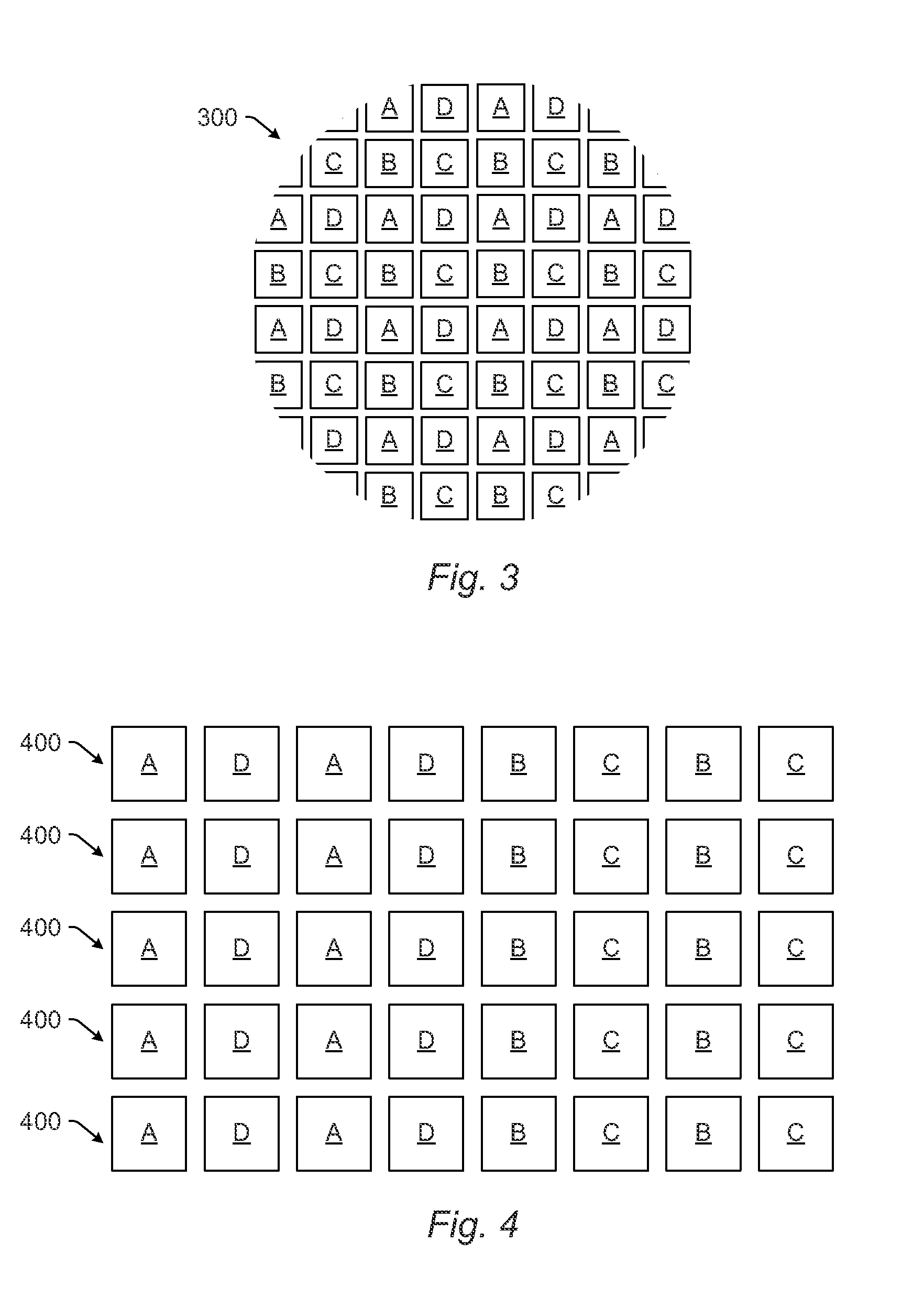
[0024]Turning now to the drawings, it is noted that the figures are not drawn to scale. In particular, the scale of some of the elements of the figures is greatly exaggerated to emphasize characteristics of the elements. It is also noted that the figures are not drawn to the same scale. Elements shown in more than one figure that may be similarly configured have been indicated using the same reference numerals. Unless otherwise noted herein, any of the elements described and shown may include any suitable commercially available elements.

[0025]One embodiment relates to a computer-implemented method for detecting defects on a wafer. The embodiments described herein provide methods and systems for identifying systematic pattern failures in effective ways using a modulated wafer layout. New wafer layouts are introduced here to decrease noise in data, increase the probability of detecting real defects, and enhance the ability to identify real systematic defects once they are reviewed on ...


PUM


Abstract

Methods and systems for detecting defects on a wafer are provided. One method includes acquiring output for a wafer generated by an inspection system. Different dies are printed on the wafer with different process conditions. The different process conditions correspond to different failure modes for the wafer. The method also includes comparing the output generated for a first of the different dies printed with the different process conditions corresponding to a first of the different failure modes with the output generated for a second of the different dies printed with the different process conditions corresponding to a second of the different failure modes opposite to the first of the different failure modes. In addition, the method includes detecting defects on the wafer based on results of the comparing step.

Description

BACKGROUND OF THE INVENTION[0001]1. Field of the Invention[0002]This invention generally relates to methods and systems for pattern failure discovery using comparisons of dies printed on a wafer with alternating failure modes for the wafer.[0003]2. Description of the Related Art[0004]The following description and examples are not admitted to be prior art by virtue of their inclusion in this section.[0005]Inspection processes are used at various steps during a semiconductor manufacturing process to detect defects on wafers to promote higher yield in the manufacturing process and thus higher profits. Inspection has always been an important part of fabricating semiconductor devices. However, as the dimensions of semiconductor devices decrease, inspection becomes even more important to the successful manufacture of acceptable semiconductor devices because smaller defects can cause the devices to fail.[0006]In general, semiconductor fabrication processes involve printing multiple dies on...

Claims


Application Information

Patent Timeline
IPC IPC(8): G06T7/00
CPCG06T7/001G06T2207/30148H01L21/67288H01L22/12H01L22/20
Inventor PARK, ALLEN
Owner KLA TENCOR TECH CORP
Why Eureka
Try Eureka