
Circuit board, and semiconductor device having component mounted on circuit board

a circuit board and semiconductor technology, applied in the direction of catalyst application resistance, sustainable manufacturing/processing, catalyst manufacturing, etc., can solve the problems of poor connection and reduce the reliability of the semiconductor device, and achieve the effect of improving the mountability of a component, improving the adhesion of solder to the pad section, and stabilizing the speed of transmission of signals

Active Publication Date: 2015-06-04
PANASONIC CORP
View PDF15 Cites 5 Cited by
  • Summary
  • Abstract
  • Description
  • Claims
  • Application Information

AI Technical Summary

Benefits of technology

[0007]As shown in FIG. 5D, it is often the case that the circuit d includes a wiring section e and a pad section f, and a component x, such as a semiconductor chip, is mounted on the pad section f via a solder bump. However, because the surface of the circuit d has been polished by CMP processing, the surface of the wiring section e and the surface of the pad section f have also been planarized and thus are very smooth. Consequently, there is a possibility that the adhesion of solder to the pad section f might be reduced, causing a poor connection and reducing the reliability of the semiconductor device.
[0008]In view of the above, it is a primary object of the present invention to improve the adhesion of solder to a pad section of an electric circuit provided in the surface of a circuit board, as well as improving the mountability of a component on the circuit board. Other objects of the present invention will be apparent as the following description of the configuration and effects of the present invention proceeds.

Problems solved by technology

Consequently, there is a possibility that the adhesion of solder to the pad section f might be reduced, causing a poor connection and reducing the reliability of the semiconductor device.

Method used


Image

  • Circuit board, and semiconductor device having component mounted on circuit board
  • Circuit board, and semiconductor device having component mounted on circuit board
  • Circuit board, and semiconductor device having component mounted on circuit board

Examples


embodiment 2

[0146]The present invention relates to a method for manufacturing a circuit board and a circuit board obtained by the production method.

[0147]In electric equipment such as portable information terminal devices, e.g., mobile phones; computers and peripherals therefor; various types of home information appliances; and the like, its functionality is being rapidly enhanced. Along with this trend, there is a growing demand for electric circuits with a further increased density in circuit boards mounted on such electric equipment. In order to meet the demand for circuits with an increased density, there is a need for methods that can precisely form electric circuit wiring having an even smaller line width and line interval (the width of a space between adjacent electric circuits). Highly densified circuit wiring is likely to cause short-circuiting, migration and the like between wires.

[0148]A known method for manufacturing a circuit board is to form an electric circuit on an insulating ba...

embodiment 2-1

[0201]A method for manufacturing a circuit board according to the present embodiment includes: a coating film forming step of forming a resin coating film on a surface of an insulating base substrate; a circuit pattern forming step of forming a circuit pattern section by forming at least either a circuit trench or hole having a desired shape and depth by laser processing or machining the insulating base substrate from an outer surface side of the resin coating film; a catalyst application step of applying a plating catalyst or precursor thereof to a surface of the circuit pattern section and a surface of the resin coating film; a coating film separation step of separating the resin coating film from the insulating base substrate; and a plating treatment step of applying an electroless plating to the insulating base substrate from which the resin coating film has been separated, wherein in the coating film forming step, an insulating base substrate with a smooth surface having a surf...

embodiment 2-2

[0273]The insulating base substrate B1 used in the coating film forming step may be obtained by pressing with a smooth plate, smooth film, smooth sheet or smooth foil. In other words, prior to the coating film forming step, a smoothing step may be performed in which at least a surface, in which the resin coating film is to be formed, of an insulating base substrate for use in the coating film forming step is smoothed. More specifically, a method for manufacturing a circuit board according to the present embodiment includes: a smoothing step of smoothing an insulating base substrate by pressing with a smooth plate, smooth film, smooth sheet or smooth foil such that at least one surface roughness Ra will be 0.5 μm or less; a coating film forming step of forming a resin coating film on the smoothed surface of the insulating base substrate; a circuit pattern forming step of forming a circuit pattern section by forming at least either a circuit trench or hole having a desired shape and d...


PUM

PropertyMeasurementUnit
wavelengthaaaaaaaaaa
particle sizeaaaaaaaaaa

Abstract

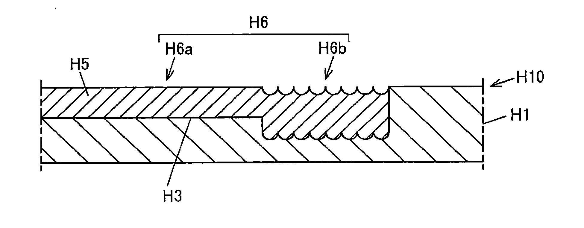
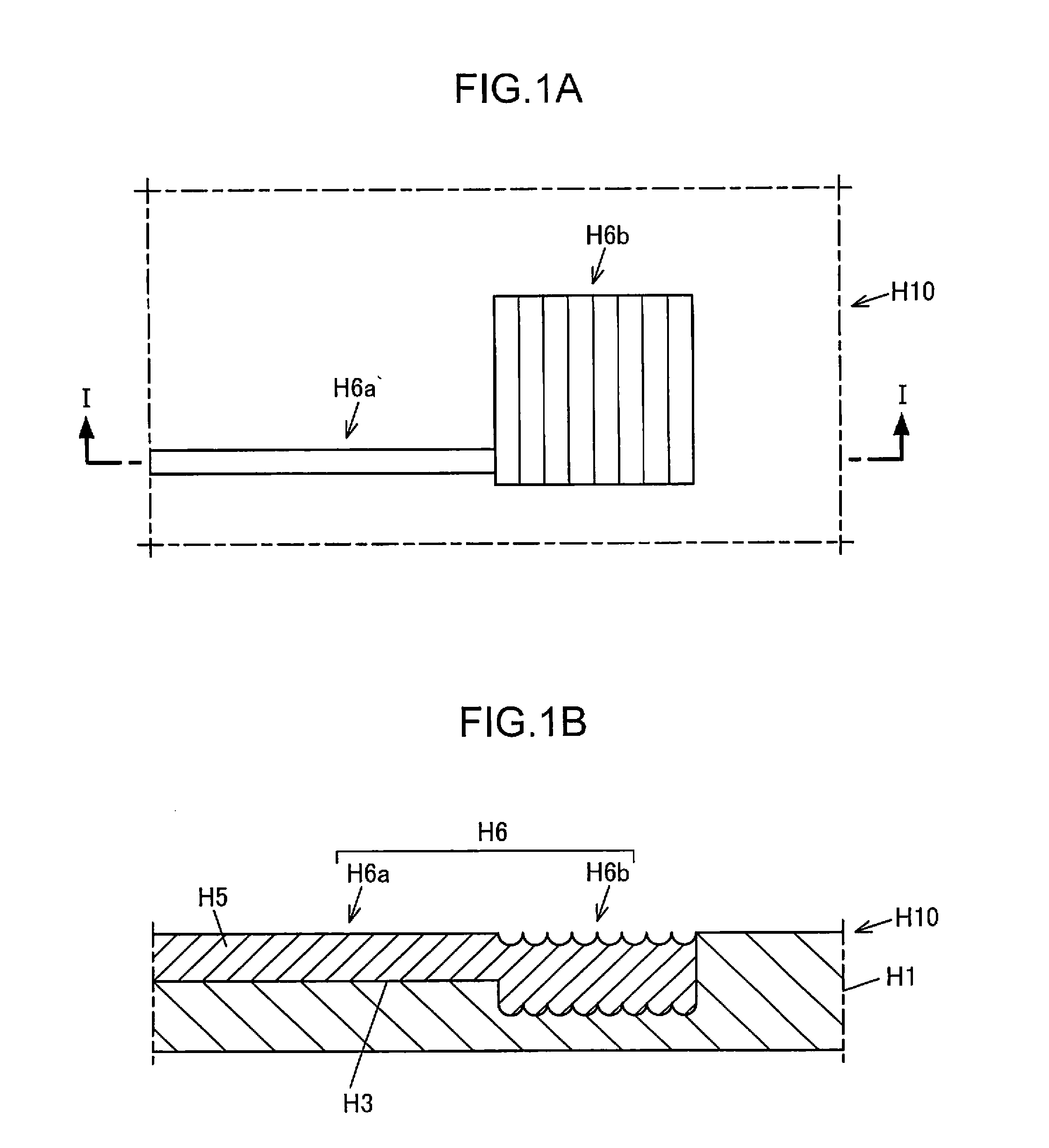
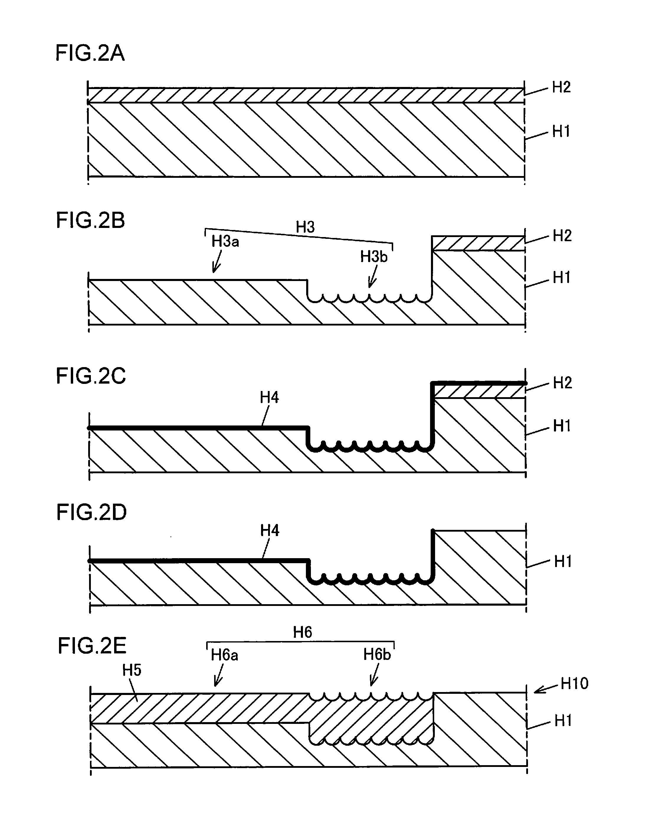
A circuit board includes an electric circuit having a wiring section and a pad section in the surface of an insulating base substrate. The electric circuit is configured such that a conductor is embedded in a circuit recess formed in the surface of the insulating base substrate, and the surface roughness of the conductor is different in the wiring section and the pad section of the electric circuit. In this case, it is preferable that the surface roughness of the conductor in the pad section is greater than the surface roughness of the conductor in the wiring section.

Description

BACKGROUND OF THE INVENTION[0001]1. Technical Field[0002]The present invention pertains to the technical field of circuit boards and semiconductor devices.[0003]2. Background Art[0004]As disclosed in, for example, Patent Document 1 (paragraph 0015), it is conventionally known that an embedded circuit forming technique using CMP (Chemical Mechanical Polishing) processing is used in a method for producing a semiconductor integrated circuit device.[0005]Specifically, as shown in FIG. 5, the circuit forming technique using CMP processing includes the steps of: forming a wiring trench (wiring groove) b in the surface of an insulating base substrate a (FIG. 5A); forming a metal member layer c on the surface of the insulating base substrate a and in the wiring trench b so as to fill the wiring trench b (FIG. 5B); and forming an embedded circuit d by removing the metal member layer c that is outside the wiring trench b by CMP processing (FIG. 5C).CITATION LISTPatent Literature[0006]Patent L...

Claims


Application Information

Patent Timeline
Patent Type & Authority Applications(United States)
IPC IPC(8): H05K1/11
CPCH05K2201/0391H05K1/111H01L21/4846H01L23/49811H01L24/16H01L24/81H01L2224/16237H01L2224/81191H01L2224/81385H01L2224/82385H01L2924/12042H01L2924/14H01L2924/3011H05K3/107H05K3/184H05K3/38H05K2201/0373H05K2201/09736H05K2201/2072H05K2203/0307H05K2203/0565Y02P70/50Y10T29/49155H01L2924/00
Inventor YOSHIOKA, SHINGOFUJIWARA, HIROAKITAKASHITA, HIROMITSUTAKEDA, TSUYOSHI
Owner PANASONIC CORP
Learn More