
Submount, encapsulated semiconductor element, and methods of manufacturing the same

a technology of encapsulated semiconductor elements and submounts, which is applied in the direction of semiconductor devices, semiconductor/solid-state device details, electrical apparatus, etc., can solve the problem of high-density submounts that cannot be manufactured, and achieve the effect of reducing parasitic capacitance, efficient electrical connection to each other, and reducing cos

Active Publication Date: 2015-04-23
ADVANCED PHOTONICS INC
View PDF1 Cites 0 Cited by
  • Summary
  • Abstract
  • Description
  • Claims
  • Application Information

AI Technical Summary

Benefits of technology

The present invention provides an improved encapsulated semiconductor element that does not require a new electrode when connecting an IC and the element on a substrate. This reduces parasitic capacitance and allows for efficient electrical connection. The electrode area is also smaller, which lowers costs. The fine pattern density is increased, making this suitable for high-density applications.

Problems solved by technology

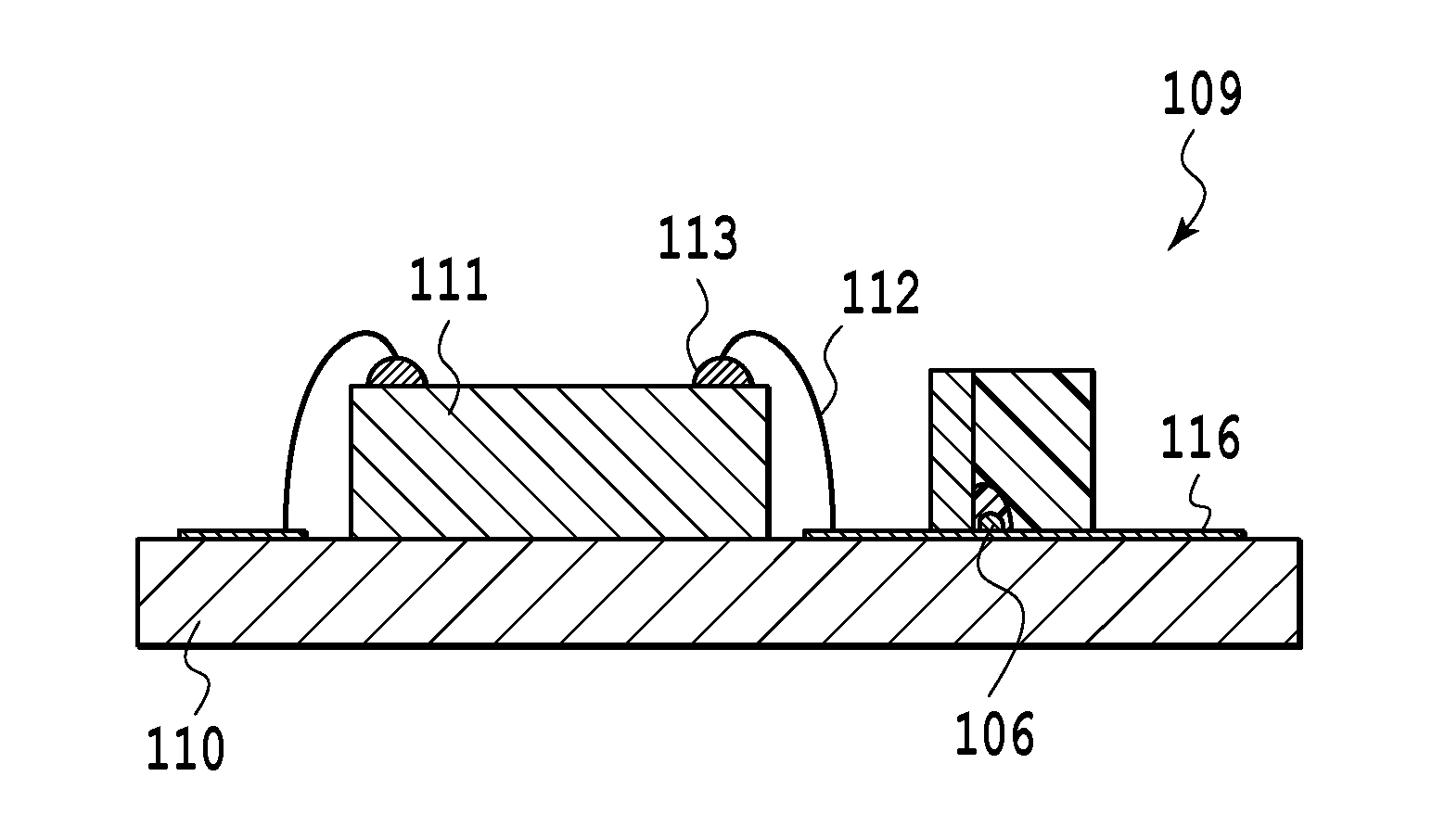
Furthermore, the module shown in FIG. 26 also includes a through-hole land portion and inevitably has a large pitch, so that there is a problem that a high-density submount cannot be manufactured.

Method used


Image

  • Submount, encapsulated semiconductor element, and methods of manufacturing the same
  • Submount, encapsulated semiconductor element, and methods of manufacturing the same
  • Submount, encapsulated semiconductor element, and methods of manufacturing the same

Examples


first embodiment

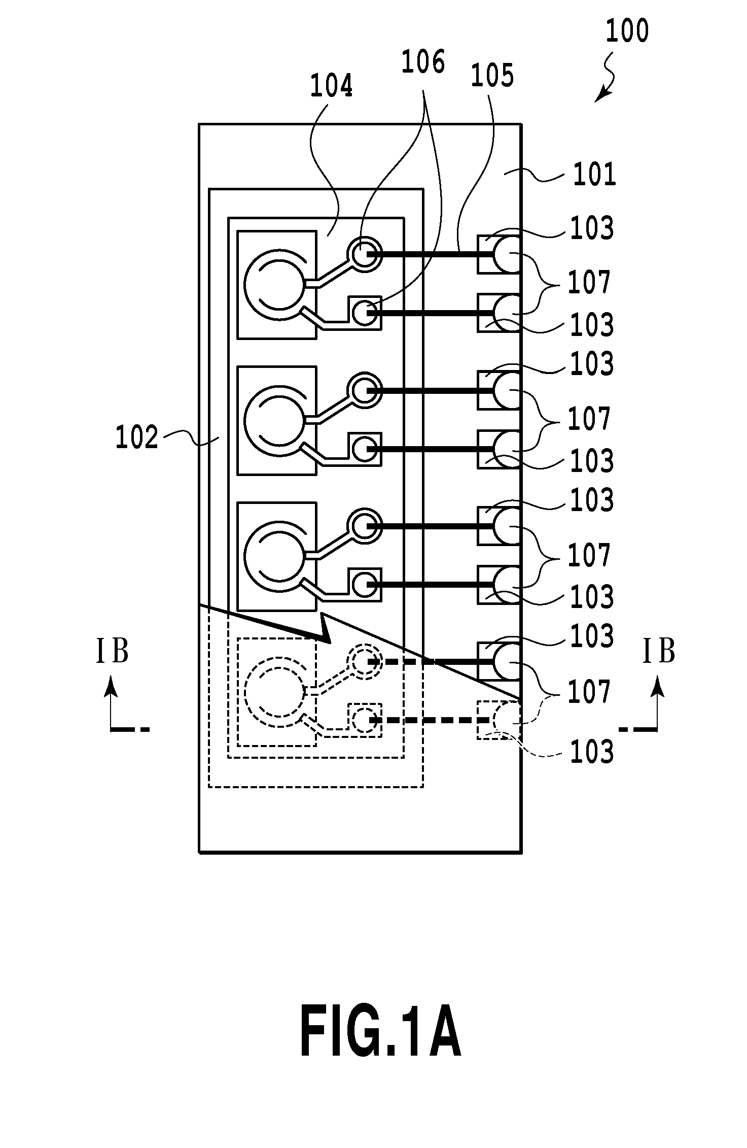
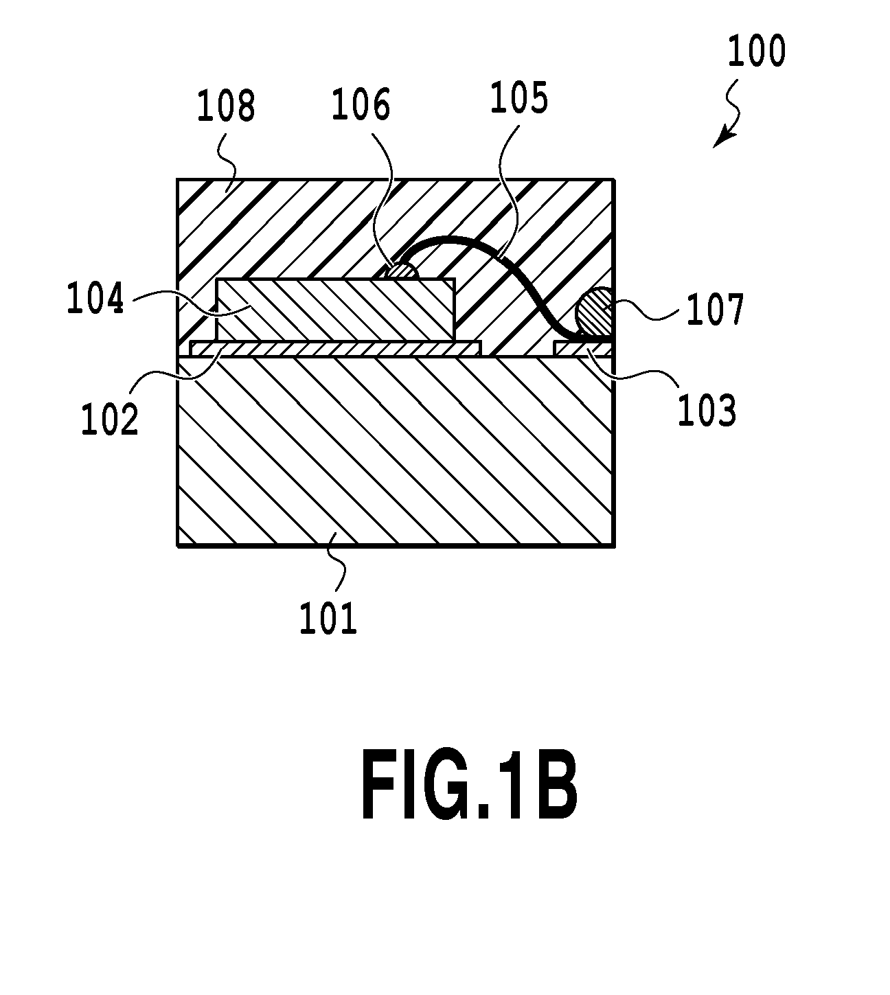
[0087]FIG. 1 includes views showing a configuration of a submount of the embodiment. FIG. 1A is a plan view of the submount. FIG. 1B is a cross-sectional view taken along the cross-section line IB-IB of FIG. 1A. For the sake of description, an upper portion of FIG. 1A is a plan view in which a resin 108 is not illustrated and a lower portion of FIG. 1A is a plan view in which the resin 108 is illustrated. Note that there are other plan views of this application which are illustrated in a similar way.

[0088]As shown in FIG. 1, the submount 100 includes a substrate 101, electrodes 102, 103, a semiconductor element 104, Au wires 105, and gold bumps 106, 107. The electrodes 102, 103, the semiconductor element 104, the Au wires 105, and the gold bumps 106, 107 are encapsulated on the substrate 101 by the resin 108.

[0089]A rigid substrate such as a glass epoxy substrate, a paper phenol substrate, a paper epoxy substrate, a glass composite substrate, a Teflon (registered trademark) substrat...

second embodiment

[0115]FIG. 6 includes views showing a configuration of a semiconductor element of the embodiment. FIG. 6A is a plan view of the semiconductor element. FIG. 6B is a cross-sectional view taken along the cross-section line VIB-VIB of FIG. 6A.

[0116]As shown in FIG. 6, gold bumps 106 are formed on a surface of the semiconductor element 104. The gold bumps 106 are encapsulated by a resin 108 on the semiconductor element 104.

[0117]The gold bumps 106 are formed on the semiconductor element 104 by ball bonding. The diameter of each gold bump 106 is preferably about 40 μm to 100 μm. As shown in FIG. 6B, the gold bumps 106 have exposed side surfaces, and these surfaces are exposed due to cut surfaces formed by dicing. A method of manufacturing the encapsulated semiconductor element including dicing and the like is described later. The exposed surfaces of the gold bumps 106 function as side surface electrodes of the encapsulated semiconductor element. Note that bumps other than the gold bumps s...

third embodiment

[0129]FIG. 9 is a view showing a configuration of a submount of the embodiment. As shown in FIG. 9, a resin 108 can be applied in such a way that gold bumps 107 are covered. The submount 100 of the embodiment is different from that of [First Embodiment] in that the resin 108 is not applied over an entire substrate 101. Since constitutional elements other than the resin 108 is the same as those of [First Embodiment], description thereof is omitted.

[0130]In the embodiment, the semiconductor element 104 is not damaged in the curing of the resin. Moreover, the amount of resin to be applied can be reduced. Note that stress due to resin curing or expansion and shrinkage of the resin caused by temperature fluctuations or the like may damage the semiconductor element.

[0131]The submount 100 of the embodiment is manufactured by forming the gold bumps 107 on electrodes 103, applying the resin 108 in such a way that the gold bumps 107 are covered, curing the applied resin 108 by heating, UV cur...


PUM


Abstract

The present invention provides a submount which includes a semiconductor element and which can be easily connected to an IC on a main substrate. The submount in one embodiment of the present invention includes: a substrate; electrodes; the semiconductor element; Au wires; and gold bumps. The electrodes, the semiconductor element, the Au wires, and the gold bumps are encapsulated on the substrate by a resin. The gold bumps are formed on the electrodes and the Au wires by ball bonding and are cut by dicing such that side surfaces of the gold bumps are exposed. The exposed surfaces function as side surface electrodes of the submount.

Description

TECHNICAL FIELD[0001]The present invention relates to a submount, an encapsulated semiconductor element, and methods for manufacturing the same.BACKGROUND ART[0002]Conventionally, in some semiconductor modules in which submounts are packaged, electrodes are formed not only on an element mounting surface of the submount but also on a side surface portion of the submount.[0003]Examples of conventional techniques include a module like one shown in FIG. 26. This module 109 includes a main substrate 110, an IC 111 on the main substrate 110, and a submount 100 on the main substrate 110. The submount 100 includes a semiconductor element 104 on an element mounting surface.[0004]In the module shown in FIG. 26, a through-hole electrode and an element mounting electrode are formed as an electrode 102 in the submount 100. An electrical connection between the IC 111 and the semiconductor element 104 is achieved by connecting the IC 111 and the electrode 102 by an AU wire 112.[0005]However, in th...

Claims


Application Information

Patent Timeline
Patent Type & Authority Applications(United States)
IPC IPC(8): H01L23/00
CPCH01L24/17H01L2924/01079H01L24/49H01L21/561H01L23/13H01L23/3114H01L23/3121H01L23/3135H01L23/49805H01L24/05H01L24/45H01L24/48H01L24/85H01L25/03H01L25/0655H01L25/0657H01L2224/03334H01L2224/0401H01L2224/04042H01L2224/05552H01L2224/05644H01L2224/05647H01L2224/05669H01L2224/06155H01L2224/13144H01L2224/16105H01L2224/16108H01L2224/16145H01L2224/16225H01L2224/16227H01L2224/1714H01L2224/45015H01L2224/45124H01L2224/45144H01L2224/45147H01L2224/45169H01L2224/48091H01L2224/48137H01L2224/48157H01L2224/48227H01L2224/48465H01L2224/48471H01L2224/48479H01L2224/48496H01L2224/48639H01L2224/48644H01L2224/48647H01L2224/48655H01L2224/48664H01L2224/48666H01L2224/48669H01L2224/48739H01L2224/48744H01L2224/48747H01L2224/48755H01L2224/48764H01L2224/48766H01L2224/48769H01L2224/48839H01L2224/48844H01L2224/48847H01L2224/48855H01L2224/48864H01L2224/48866H01L2224/48869H01L2224/48997H01L2224/4911H01L2224/49175H01L2224/73207H01L2224/73265H01L2224/81193H01L2224/85395H01L2224/85439H01L2224/85444H01L2224/85447H01L2224/85455H01L2224/85464H01L2224/85466H01L2224/8592H01L2224/94H01L2224/97H01L2225/0651H01L2225/06513H01L2225/06551H01L2225/06562H01L2225/06575H01L2924/00014H01L2924/01015H01L2924/01047H01L2924/12042H01L2924/14H01L2924/15153H01L2924/15159H01L2924/157H01L2924/15787H01L2924/15788H01L2924/181H01L2924/30107H01L2924/3011H01L2224/03H01L2224/85H01L2924/00H01L2224/48455H01L2924/00012H01L2224/4554
Inventor SONG, XUELIANGSATO, NOZOMUKANNO, GENTAMAKINO, YOHKO
Owner ADVANCED PHOTONICS INC
Learn More