Image processing apparatus and control method thereof
- Summary
- Abstract
- Description
- Claims
- Application Information
AI Technical Summary
Benefits of technology
Problems solved by technology
Method used
Image
Examples
first embodiment
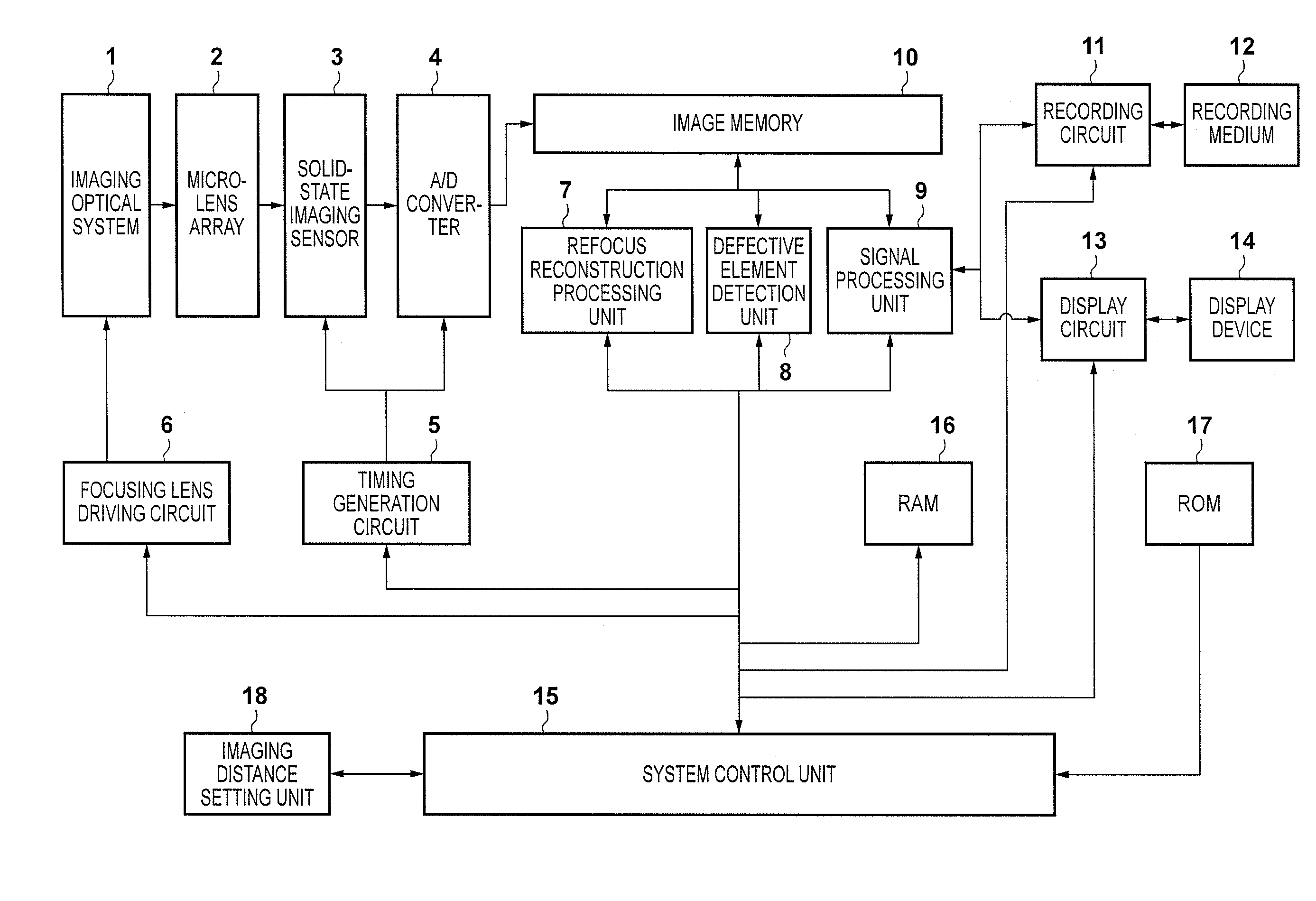
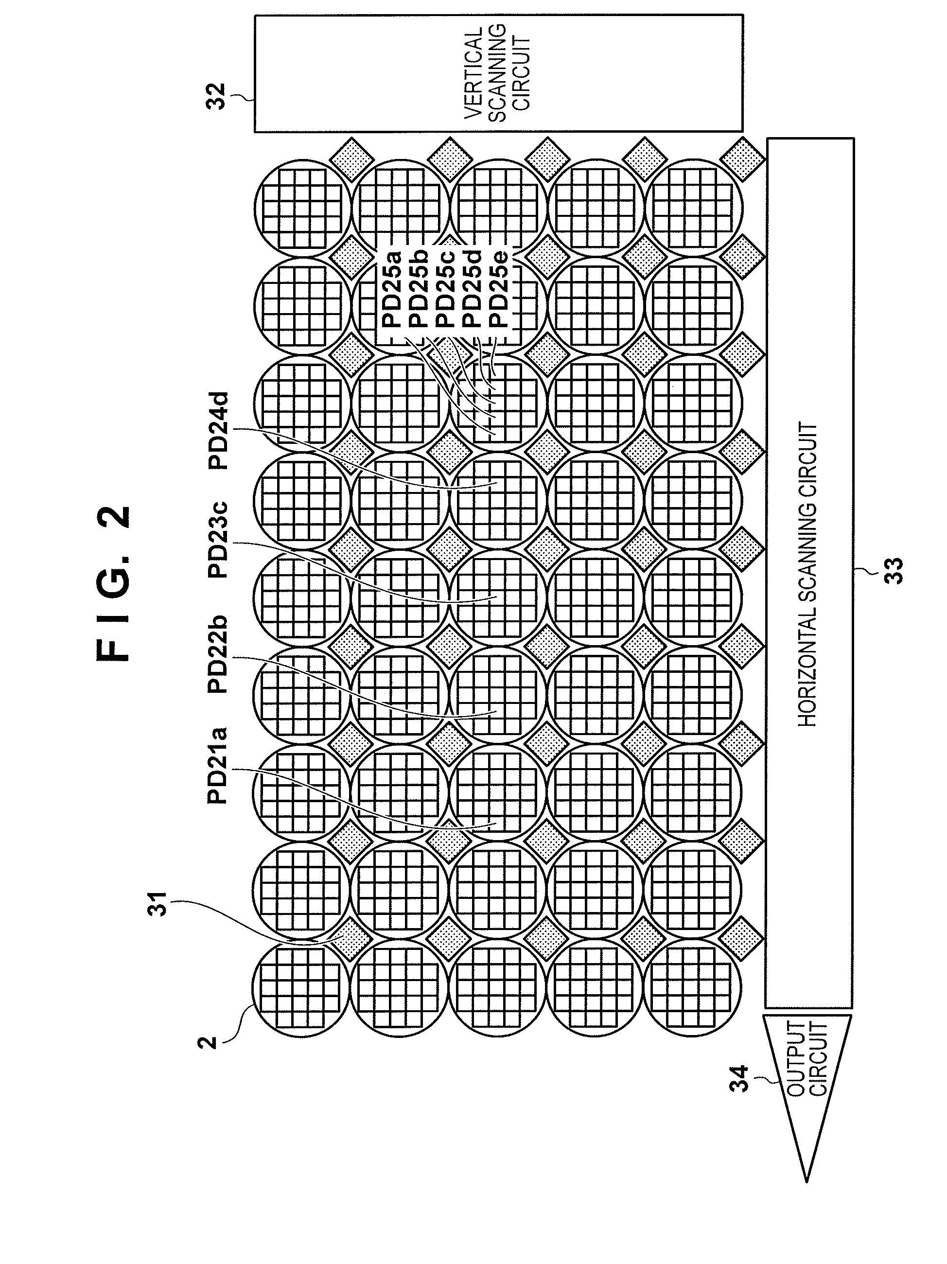
[0031]FIG. 1 is a block diagram showing the overall arrangement of an image capturing apparatus according to the first embodiment of the present invention. In FIG. 1, an imaging optical system 1 includes a stop and focusing lens, and forms the optical image of an object. Microlens arrays 2 form images of an object through the focusing lens of the imaging optical system 1 at mainly their vertices. The microlens arrays 2 are two-dimensionally arrayed at a predetermined pitch in the horizontal and vertical directions. A solid-state imaging sensor 3 photoelectrically converts an object image formed by the imaging optical system 1, and extracts it as an electrical signal. The solid-state imaging sensor 3 has the function of a photoelectric conversion element that is implemented by pixels two-dimensionally arranged in the horizontal and vertical directions at a pitch smaller than the pitch of the microlens arrays 2. The solid-state imaging sensor 3 also has a signal transfer function of t...
second embodiment
[0089]In the second embodiment, a defective element extraction error is reduced by performing defective pixel detection processing on a larger number of reconstructed images.
[0090]Prior to a description of the second embodiment, it will be explained first that a defective element cannot be completely specified from only two reconstructed images, as in the first embodiment, and a defective element extraction error may occur.
[0091]FIG. 7 is a light beam view for explaining defective element address extraction processing. For descriptive convenience, defective element address extraction processing will be explained by giving attention to pixels arranged in one direction, microlens arrays 2, and five elements arranged for every unit microlens array 2. In FIG. 7, pixels 53 and 55 of a reconstructed image 41, and pixels 63 and 65 of a reconstructed image 42 are pixels detected as defective pixels through real-time defective pixel detection steps S308 and S311 in FIG. 3.
[0092]In this case,...
third embodiment
[0107]The first and second embodiments have described the fact that a defective element can be logically extracted from a real-time defective pixel detection result on the assumption that “a pixel obtained by adding signals including at least the signal of a defective element is detected as a defective pixel”. However, it is readily considered that “a pixel obtained by adding signals including the signal of a defective element is not always detected as a defective pixel” in practice owing to various factors. Examples of these factors are optical shot noise, circuit noise of a solid-state imaging sensor, the output signal intensity and imaging distance of a defective element, and a detection error and no detection in real-time defective pixel detection.
[0108]The third embodiment will explain a method of appropriately extracting a defective element from a plurality of reconstructed images without specifying a defective element by real-time defective pixel detection. In the third embod...
PUM
 Abstract
Description
Claims
Application Information
 - R&D
- Intellectual Property
- Life Sciences
- Materials
- Tech Scout
- Unparalleled Data Quality
- Higher Quality Content
- 60% Fewer Hallucinations
Browse by: Latest US Patents, China's latest patents, Technical Efficacy Thesaurus, Application Domain, Technology Topic, Popular Technical Reports.
© 2025 PatSnap. All rights reserved.Legal|Privacy policy|Modern Slavery Act Transparency Statement|Sitemap|About US| Contact US: help@patsnap.com


