Electromagnetic wave propagation disruption device and method for producing same
- Summary
- Abstract
- Description
- Claims
- Application Information
AI Technical Summary
Benefits of technology
Problems solved by technology
Method used
Image
Examples
Embodiment Construction
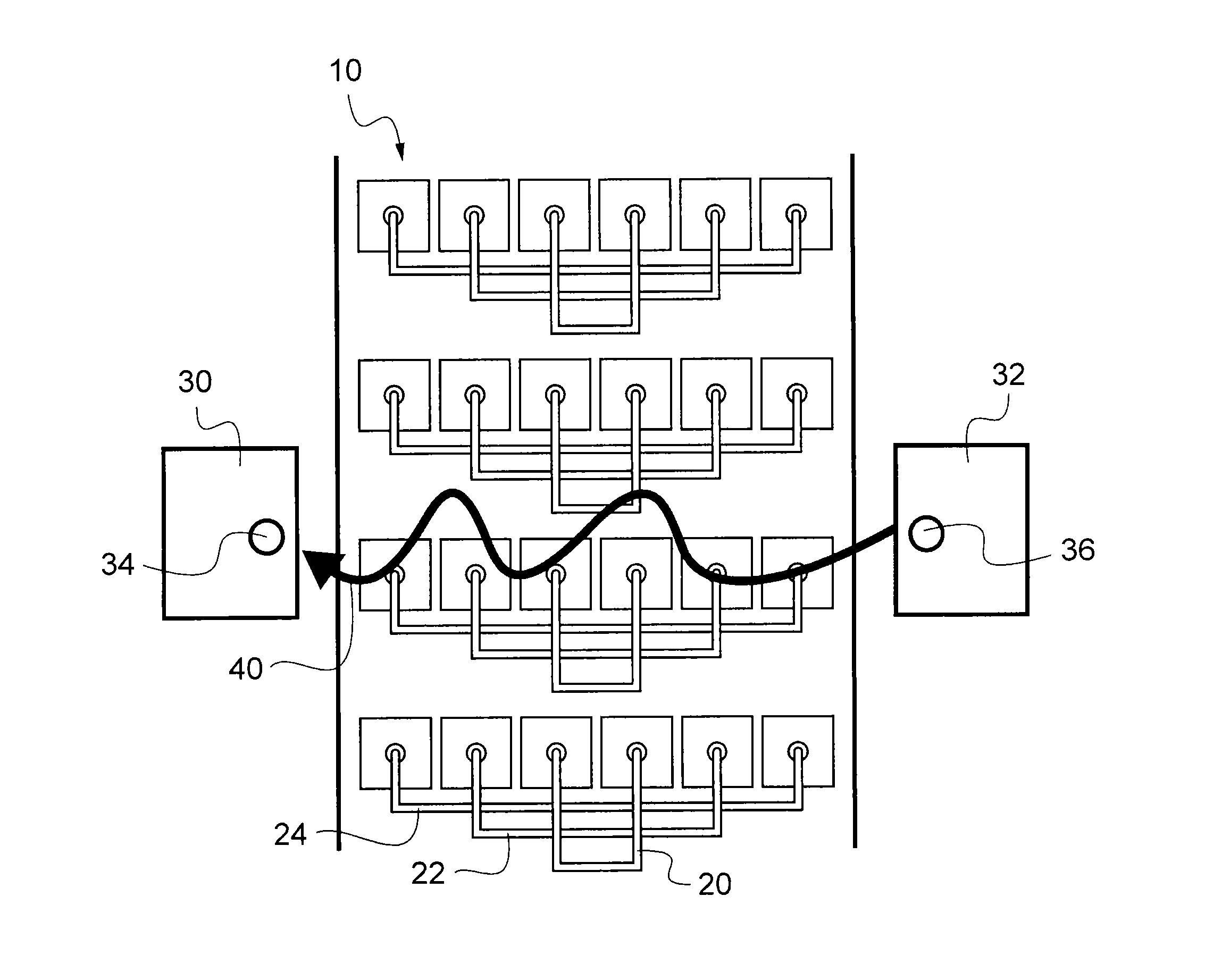
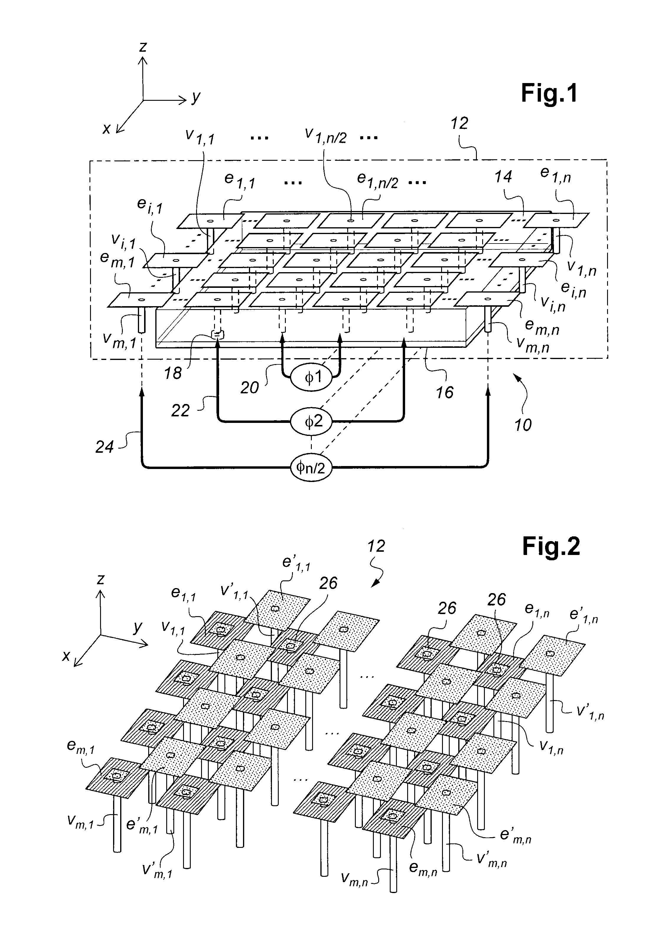
[0052]FIG. 1 represents a sectional perspective view of the overall structure of an electromagnetic wave propagation disruption device 10 with a metamaterial structure 12, according to one possible embodiment of the invention. This device may for example be positioned between two elements of a planar antenna defined on the same substrate to limit the surface waves between these two elements.
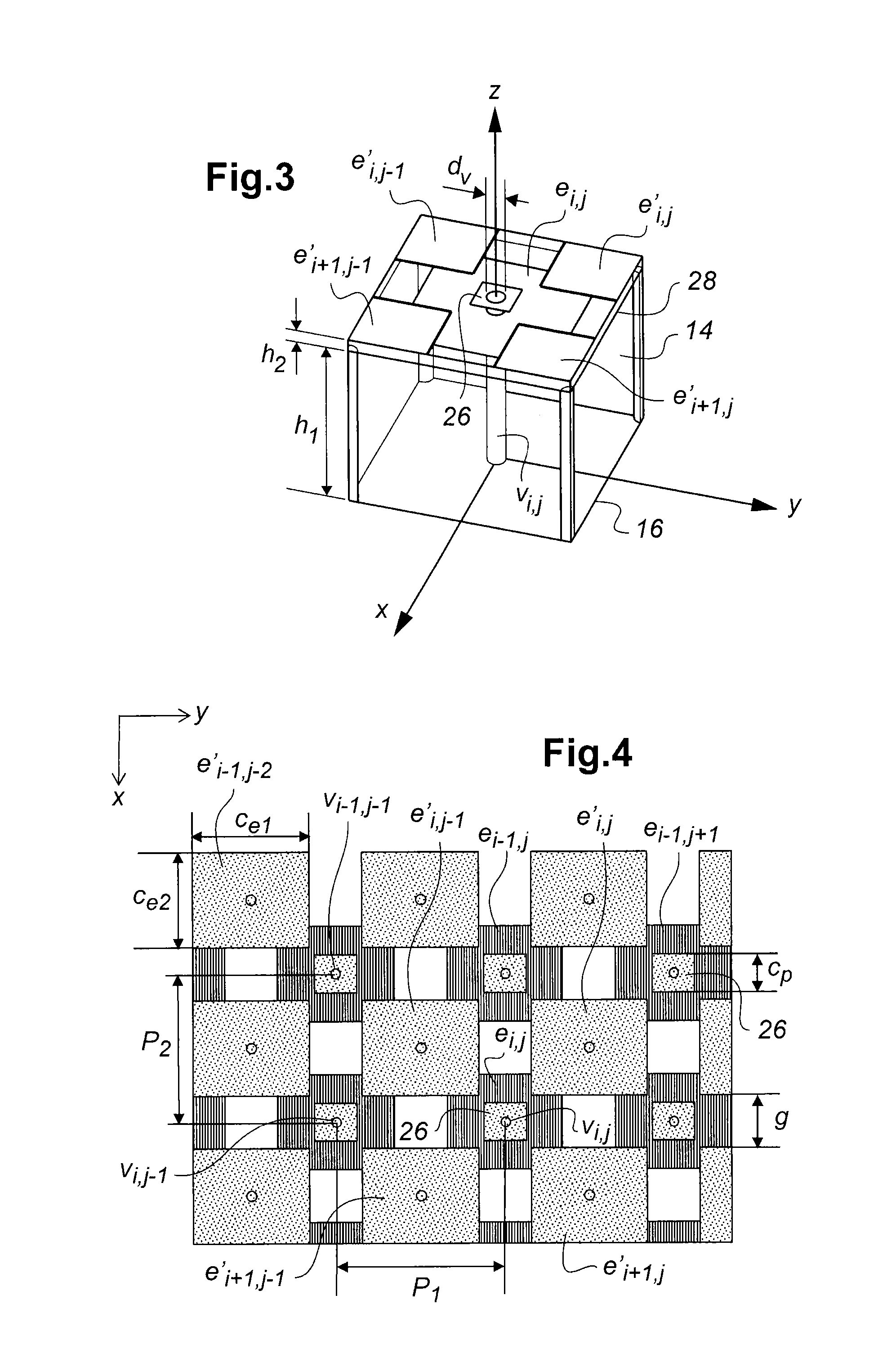
[0053]In this embodiment, the metamaterial structure 12 is of the mushroom type and comprises a plurality of conductive elements e1,1, . . . , ei,j, . . . , em,n in a rectangular shape, separated from each other and arranged on a top face of a substrate 14 made, for example, of dielectric material. This substrate may be an epoxy-based insulating material, an insulating material well known to those skilled in the art, for example FR4 type with a relative permittivity value εR of approximately 4.4. The conductive elements e1,1, . . . , ei,j, . . . , em,n are distributed on the substrate 14 in an ar...
PUM
| Property | Measurement | Unit |
|---|---|---|
| Electrical conductor | aaaaa | aaaaa |
Abstract
Description
Claims
Application Information
 - R&D
- Intellectual Property
- Life Sciences
- Materials
- Tech Scout
- Unparalleled Data Quality
- Higher Quality Content
- 60% Fewer Hallucinations
Browse by: Latest US Patents, China's latest patents, Technical Efficacy Thesaurus, Application Domain, Technology Topic, Popular Technical Reports.
© 2025 PatSnap. All rights reserved.Legal|Privacy policy|Modern Slavery Act Transparency Statement|Sitemap|About US| Contact US: help@patsnap.com


