
High-energy ion implanter

Active Publication Date: 2014-12-04
SUMITOMO HEAVY IND ION TECH
View PDF2 Cites 11 Cited by
  • Summary
  • Abstract
  • Description
  • Claims
  • Application Information

AI Technical Summary

Benefits of technology

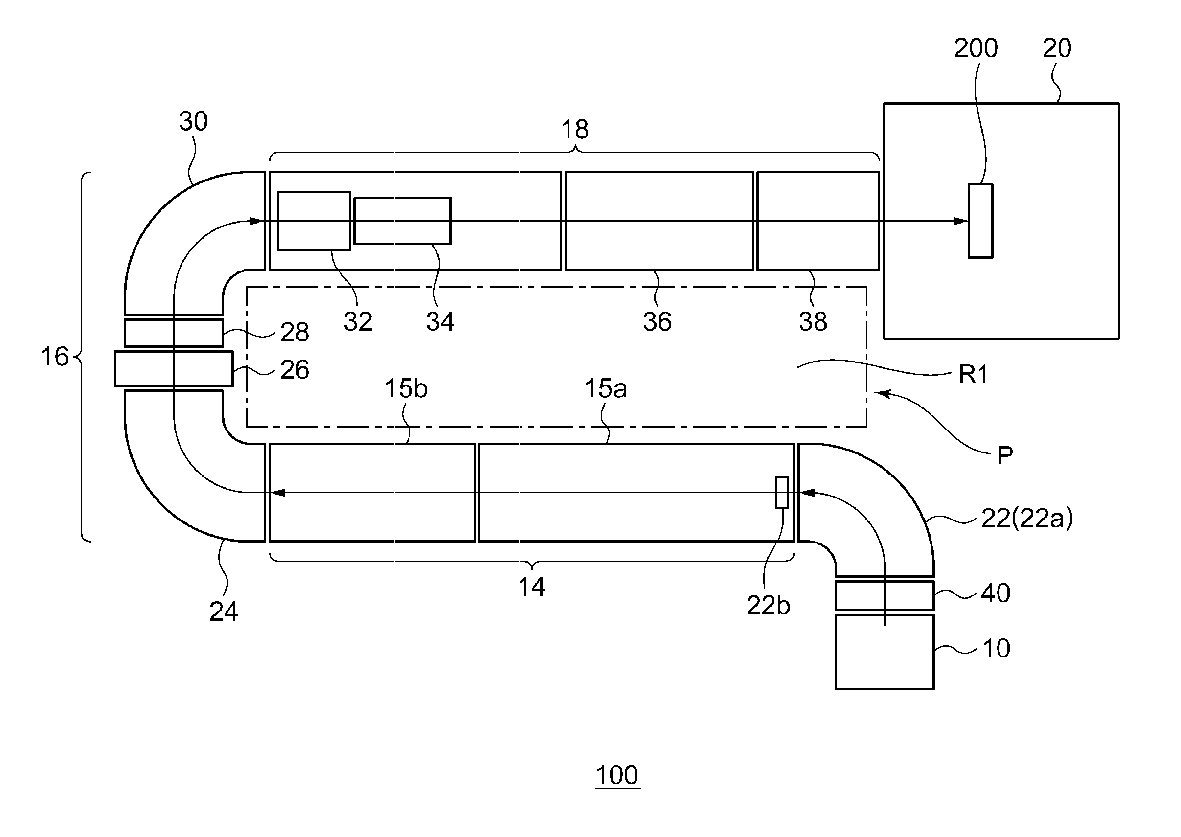
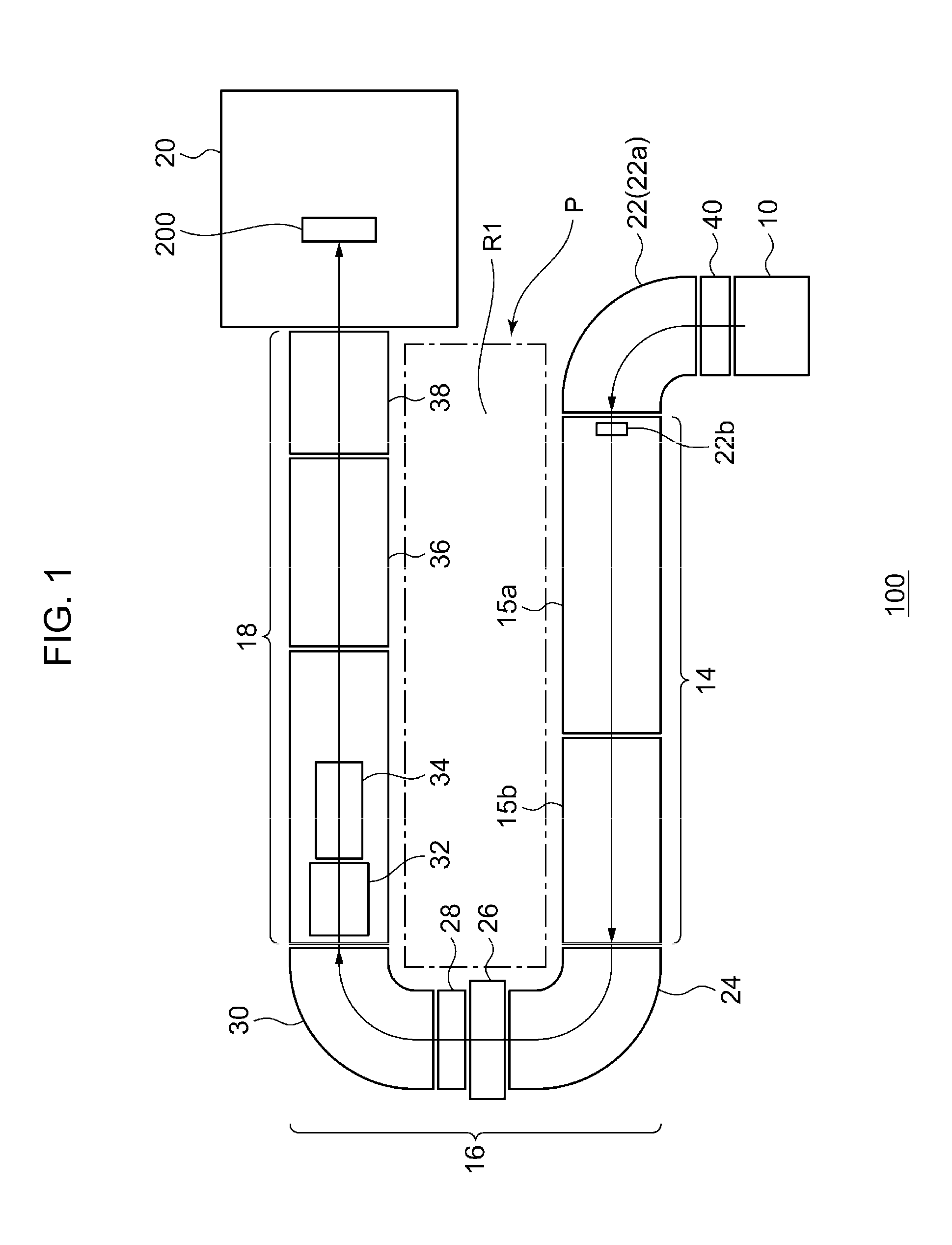
The invention is a high-energy ion implanter that can scan and deflect a high-energy ion beam. It includes a beam generation unit, a high-energy multi-stage linear acceleration unit, a beam deflection unit, a beam transportation unit, and a substrate processing / supplying unit. The beam transportation unit includes a beam shaper, a high-energy beam scanner, a high-energy electric field type beam collimator, and a high-energy electric field type final energy filter. The high-energy ion beam emitted from the deflection unit is scanned and collimated, and the resultant ions are implanted into the wafer. The technical effect of the invention is to provide a more efficient and accurate method for ion implantation into semiconductor wafers.

Problems solved by technology

The batch treatment type ion implantation method has a problem in which an implantation angle (an angle at which the ions are incident to the wafer) is different by about 1° between the center and the end of the wafer (the implantation angle deviation) due to the above-described angle and the rotation of the wafer.

Method used


Image

  • High-energy ion implanter
  • High-energy ion implanter
  • High-energy ion implanter

Examples


Embodiment Construction

[0038]The invention will now be described by reference to the preferred embodiments. This does not intend to limit the scope of the present invention, but to exemplify the invention.

[0039]Hereinafter, an example of a high-energy ion implanter according to the embodiment will be described in detail. First, the reason why the invention is contrived by the present inventor and the like will be described.

[0040](Parallel Magnet)

[0041]The following problems arise in a high-energy ion implanter of the related art that employs a parallel (collimate) magnet which parallelizes (collimates) an orbit by a deflection magnetic field.

[0042]When a high-energy ion is implanted into a photoresist-coated wafer, a large amount of an outgas is generated. Then, an interaction occurs between molecules of the outgas and beam ions, and hence the charge state of some ions change. When a change in valance occurs while the beam passes through the parallel magnet, a deflection angle changes and the parallelism ...


PUM

PropertyMeasurementUnit
frequencyaaaaaaaaaa
deflection angleaaaaaaaaaa

Abstract

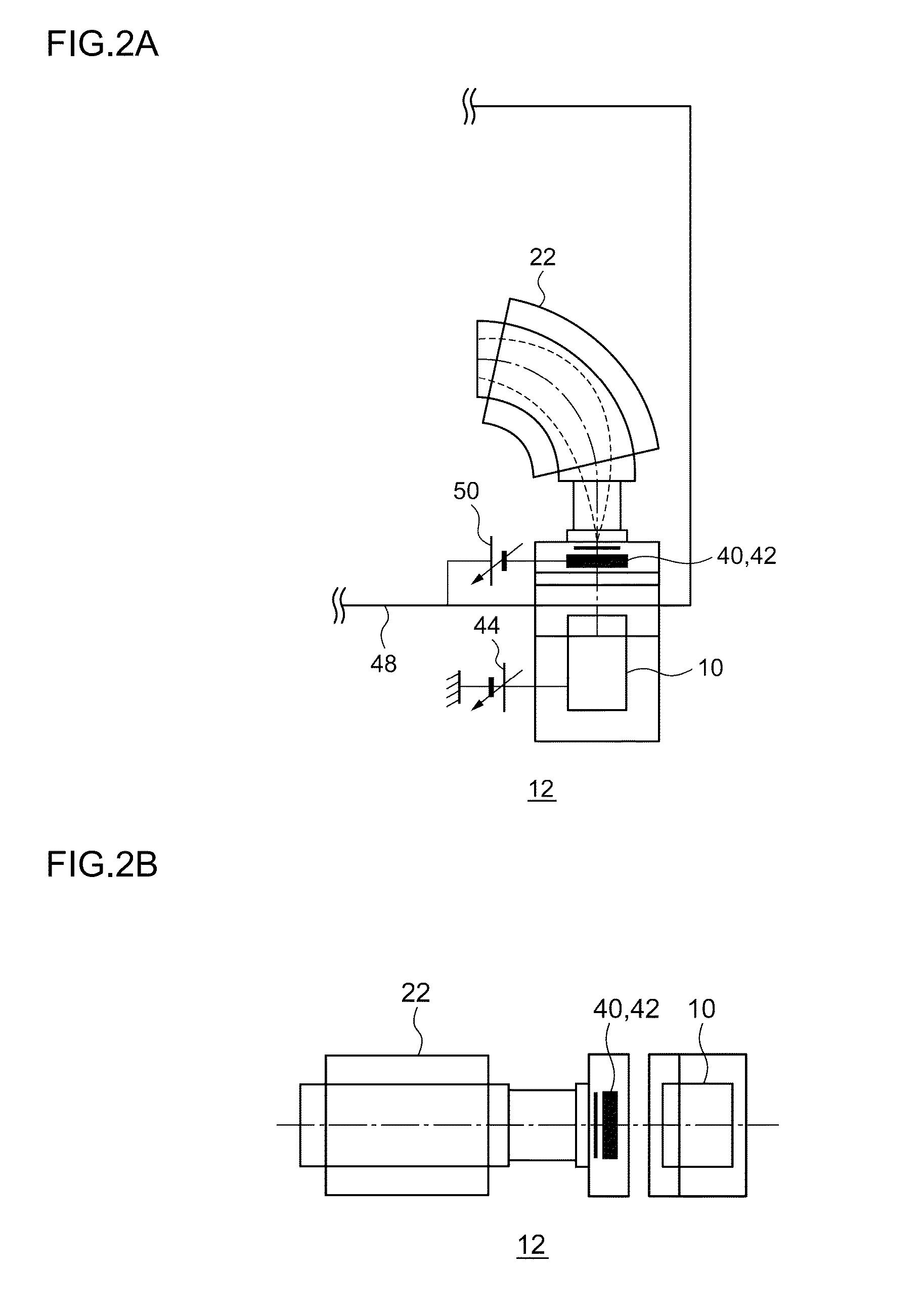
A high-energy ion implanter includes a high-energy multi-stage linear acceleration unit that accelerates an ion beam so as to generate a high-energy ion beam, a deflection unit that changes the direction of the high-energy ion beam toward a semiconductor wafer, and a beam transportation unit that transports the deflected high-energy ion beam to the wafer. The beam transportation unit includes a beam shaper, a high-energy beam scanner, a high-energy electric field type beam collimator, and a high-energy electric field type final energy filter.

Description

BACKGROUND OF THE INVENTION[0001]1. Field of the Invention[0002]The present invention relates to a high-energy ion implanter.[0003]2. Description of the Related Art[0004]In a semiconductor device production process, an important process is generally performed in which ions are implanted into a semiconductor wafer in a vacuum state so as to add impurities to crystals of the semiconductor wafer. Accordingly, a conductive property is changed so that the semiconductor wafer becomes a semiconductor device. An apparatus used in this process is generally called an ion implanter that accelerates impurity atoms as ions for the semiconductor device and implants impurity atoms into the semiconductor wafer.[0005]Hitherto, an apparatus for performing a high-energy ion implantation by further deeply implanting an ion beam into the semiconductor wafer has been used with the high integration and the high performance of the semiconductor device. Such an apparatus is particularly called a high-energy...

Claims


Application Information

Patent Timeline
Patent Type & Authority Applications(United States)
IPC IPC(8): C23C14/48
CPCC23C14/48H01J37/3171H01J2237/1518H05H7/04H05H9/045H05H2007/046
Inventor KABASAWA, MITSUAKIWATANABE, KAZUHIROSASAKI, HARUKAINADA, KOUJI
Owner SUMITOMO HEAVY IND ION TECH
Learn More