Diffractive optics element, method for manufacturing diffractive optics element, and electronic device

a diffractive optics and element technology, applied in the field of diffractive optics elements, diffractive optics elements, method for manufacturing diffractive optics elements, electronic devices, etc., can solve the problems of thermal deformation, discoloration, and original performance cannot be maintained for a short time, so as to improve display quality and increase heat resistance

Active Publication Date: 2014-11-27
SEIKO EPSON CORP
View PDF8 Cites 2 Cited by
  • Summary
  • Abstract
  • Description
  • Claims
  • Application Information

AI Technical Summary

Benefits of technology

This patent describes a diffractive optics element made of a very thin material that takes a siloxane bond as its skeleton, which helps to suppress the emission of heat when it is exposed to a high-output laser beam. The heat produced by the diffractive optics portion is quickly dissipated through a short heat path to the transparent substrate, resulting in a minimal temperature rise of the diffractive optics element. This design provides a high reliability and lifespan for the diffractive optics element. Additionally, by using a material that takes a siloxane bond as its skeleton, which is highly heat resistant, the lifespan and reliability of the diffractive optics element can be improved. This results in an electronic device that has increased heat resistance, improved display quality, and other benefits.

Problems solved by technology

However, in the case where, for example, a thermosetting resin is used as the hologram layer, there is a problem in that because the resin has a low heat resistance temperature, a high-output laser beam for a high light flux projector being incident thereon will result in thermal deformation, discoloration, and so on, and as a result, the original performance can only be maintained for a short amount of time.
There is a further problem in that it is necessary to ensure both a high level of transmissibility that can withstand even a high-output laser beam and a high level of heat resistance that can withstand heat generated when laser light is absorbed.

Method used


Image

  • Diffractive optics element, method for manufacturing diffractive optics element, and electronic device
  • Diffractive optics element, method for manufacturing diffractive optics element, and electronic device
  • Diffractive optics element, method for manufacturing diffractive optics element, and electronic device

Examples


first embodiment

Configuration of Projector Serving as Electronic Device

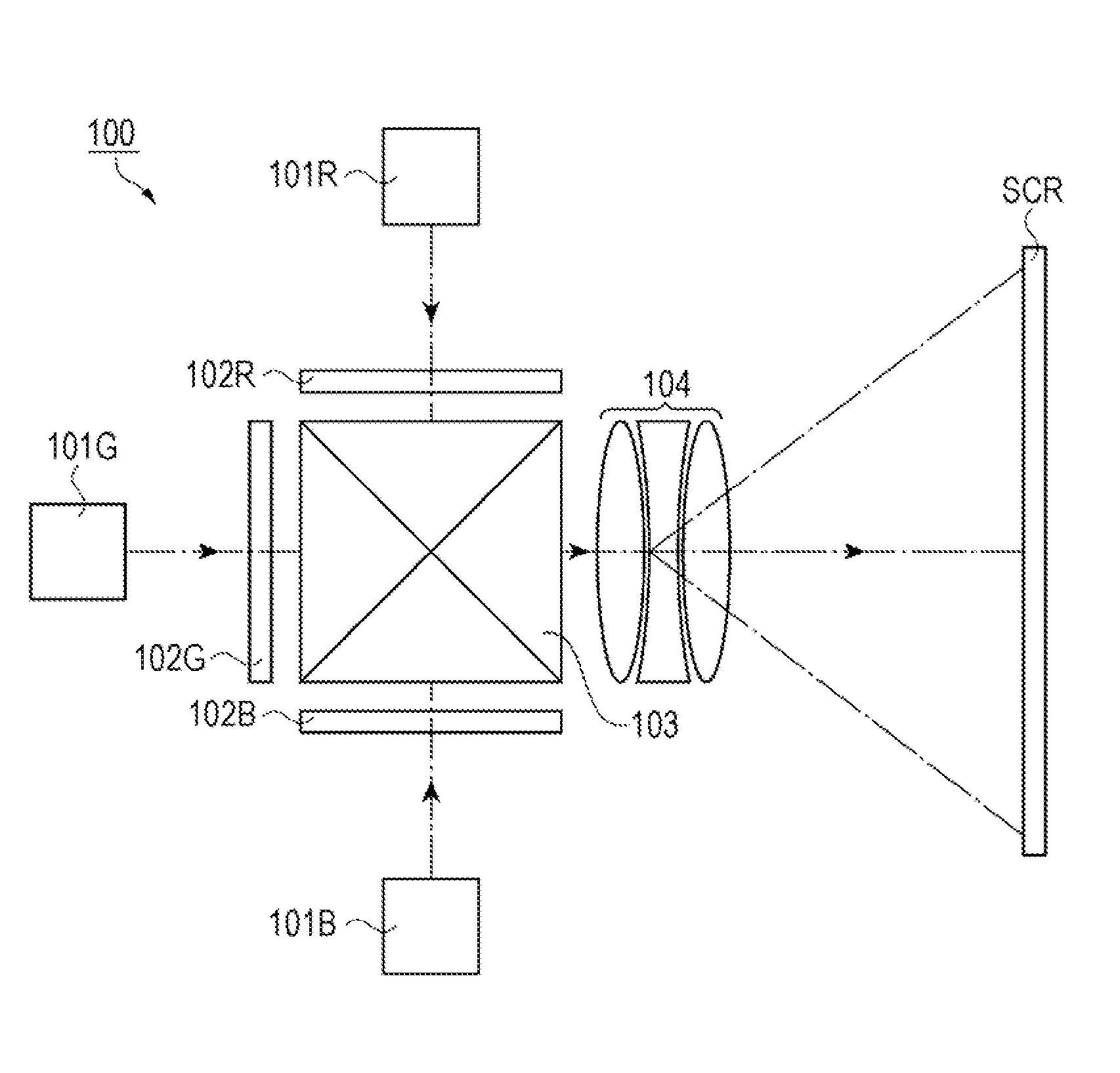
[0032]FIG. 1 is a schematic diagram illustrating the configuration of a projector that serves as an electronic device and includes a diffractive optics element. The configuration of the projector will be described hereinafter with reference to FIG. 1.

[0033]As shown in FIG. 1, a projector 100 is a projection-type image display apparatus that displays color pictures (images) on a screen (projection surface) SCR. The projector 100 uses three liquid-crystal light valves (liquid crystal panels), one for each of red light RL, green light GL, and blue light BL, as optical modulating elements. Furthermore, the projector 100 uses a semiconductor laser (laser light source), from which high-luminosity and high-output light can be obtained, as a light source in illumination units.

[0034]Specifically, the projector 100 includes illumination units 101 (101R, 101G, and 101B), optical modulation elements 102 (102R, 102G, and 102B), a synthesizin...


PUM


Abstract

A diffractive optics element includes a substrate configured of a sapphire substrate and a diffractive optics structure, provided on the substrate, that forms an image when a laser beam is incident thereon. The diffractive optics structure has a diffractive optics portion, and the diffractive optics portion has a base material and a diffractive optics layer disposed on the base material. The thickness of the base material is no greater than 20 μm.

Description

BACKGROUND[0001]1. Technical Field[0002]The present invention relates to diffractive optics elements having surface relief holograms, methods for manufacturing such diffractive optics elements, and electronic devices.[0003]2. Related Art[0004]The stated diffractive optics element is used, for example, as part of an illumination optical system in a projector. A hologram such as that disclosed in JP-A-11-161142, for example, which has a structure in which a hologram layer configured of a thermosetting resin or the like is provided upon a transparent substrate such as glass, can be given as an example of a diffractive optics element. Meanwhile, in recent years, laser light sources have begun to be used as light sources in projectors as well.[0005]A surface relief-type computer generated hologram (CGH) can be given as an example of a diffractive optics element that can configure an illumination optical system in combination with the aforementioned laser light source. A surface-relief ho...

Claims


Application Information

Patent Timeline
IPC IPC(8): G02B27/42
CPCG02B27/42G02B27/4222G02B27/4233
Inventor SORIMACHI, HIDEMITSUNOJIMA, SHIGEO
Owner SEIKO EPSON CORP
Why Eureka
Try Eureka