
Electron gun arrangement

a technology of electron gun and charge particle, which is applied in the direction of material analysis using wave/particle radiation, instruments, nuclear engineering, etc., can solve the problems of high cost, high cost, and high cost of electron gun, and achieve the effect of improving electron and improving charge particle beam

Active Publication Date: 2014-09-18
ICT INTEGRATED CIRCUIT TESTING GESELLSCHAFT FUER HALBLEITERPRUEFTECHNIK GMBH
View PDF3 Cites 17 Cited by
  • Summary
  • Abstract
  • Description
  • Claims
  • Application Information

AI Technical Summary

Benefits of technology

The present invention provides an improved electron gun arrangement and charged particle beam device with a field emitter, extractor electrode, suppressor electrode, and auxiliary emitter electrode. The invention provides an improved method of cleaning the extractor electrode and a system for wafer imaging using the electron gun arrangement. The technical effects of the invention include improved electron beam control and stability, improved electron beam quality, and more efficient and precise wafer imaging. The invention is applicable to a range of electron gun arrangements and charged particle beam devices.

Problems solved by technology

In spite of that, electrons impinging on component surfaces of the device, like extractors, anodes, apertures or the chamber wail result in an emission of contaminants.
Even though such emitters are known for a long time, implementation thereof in industrial applications, wherein a high availability of systems and high stability due to desired automation is demanded, have been experienced to be difficult due to these requirements.
Thus, it is difficult to provide a high brightness electron source for electron microscopy, such as a CFE or thermally assisted CFE, and more specifically for electron beam based wafer inspection, with sufficient stability of operation.

Method used


Image

  • Electron gun arrangement
  • Electron gun arrangement
  • Electron gun arrangement

Examples


Embodiment Construction

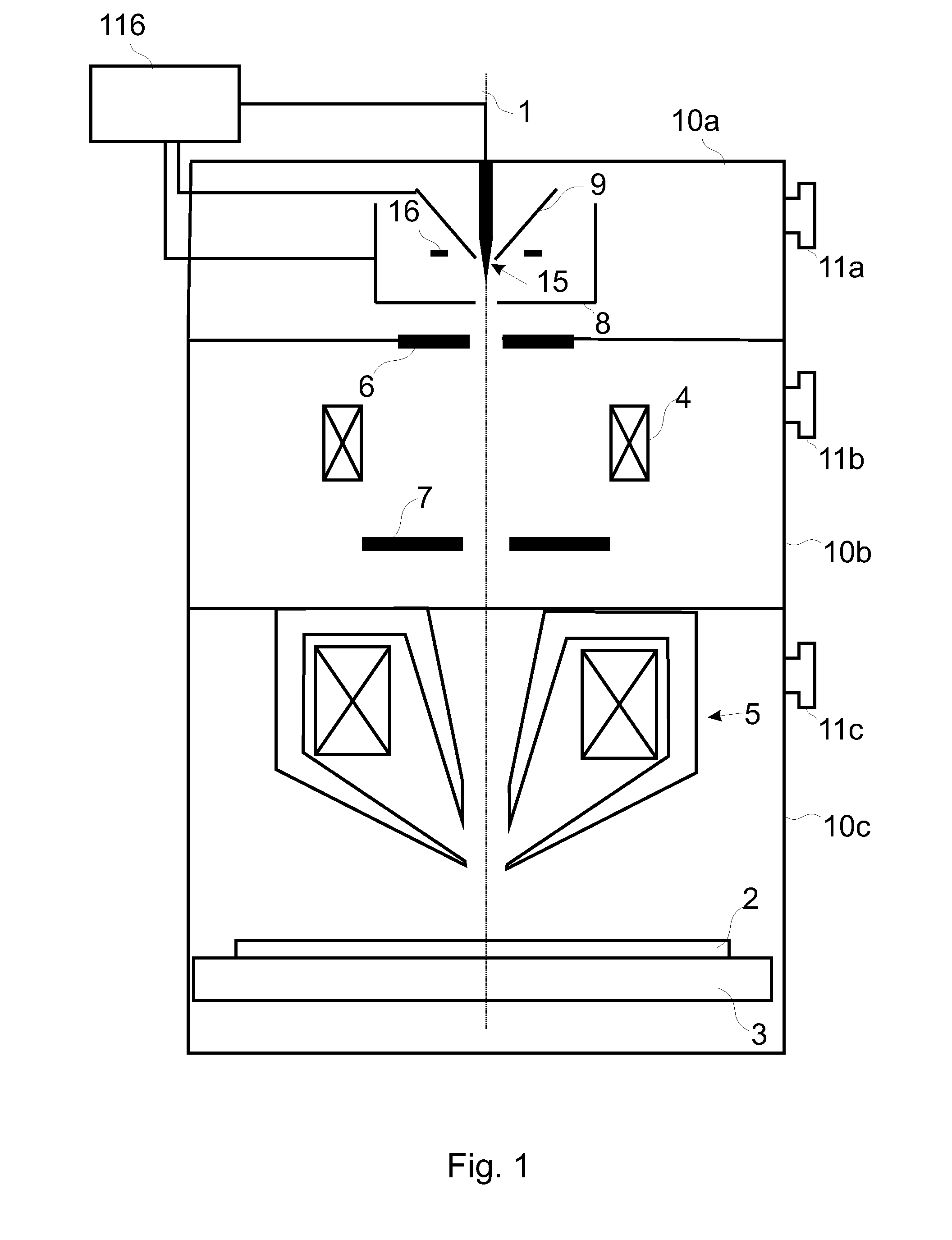
[0017]Reference will now be made in detail to the various embodiments of the invention, one or more examples of which are illustrated in the figures. Within the following description of the drawings, the same reference numbers refer to same components. Generally, only the differences with respect to individual embodiments are described. Each example is provided by way of explanation of the invention and is not meant as a limitation of the invention. Further, features illustrated or described as part of one embodiment can be used on or in conjunction with other embodiments to yield yet a further embodiment. It is intended that the description includes such modifications and variations.

[0018]Without limiting the scope of protection of the present application, in the following the charged particle beam device or components thereof will exemplarily be referred to as a charged particle beam device including the detection of secondary electrons. Embodiments of the present invention can st...


PUM


Abstract

A gun arrangement configured for generating a primary electron beam for a wafer imaging system is described. The arrangement includes a controller configured for switching between a normal operation and a cleaning operation, a field emitter having an emitter tip adapted for providing electrons and emitting an electron beam along an optical axis, an extractor electrode adapted for extracting the electron beam from the emitter tip electrode, a suppressor electrode, and at least one auxiliary emitter electrode arranged radially outside the suppressor electrode, and provided as a thermal electron emitter for thermally emitting electrons towards the optical axis.

Description

FIELD OF THE INVENTION[0001]The invention relates to a charged particle beam device for inspection system applications, testing system applications, lithography system applications, electron microscopes and the like. It also relates to methods of operation thereof. Further, the present invention relates to a charged particle beam device with a cleaning system. Specifically, it relates to a gun arrangement, a charged particle beam device, a method of cleaning and Operating a charged particle beam device, and method of cleaning a surface of an extractor electrode of an electron gun arrangement.BACKGROUND OF THE INVENTION[0002]Charged particle beam apparatuses are used in a plurality of industrial fields. Inspection of semiconductor devices during manufacturing, exposure systems for lithography, detecting devices and testing systems are only some of these fields.[0003]In general, there is a high demand for structuring and inspecting specimens within the micrometer or nanometer scale. O...

Claims


Application Information

Patent Timeline
IPC IPC(8): H01J37/02H01J37/063H01J37/24H01J37/073
CPCH01J37/026H01J37/243H01J37/063H01J37/073H01J3/027H01J2237/022
Inventor ADAMEC, PAVEL
Owner ICT INTEGRATED CIRCUIT TESTING GESELLSCHAFT FUER HALBLEITERPRUEFTECHNIK GMBH
Learn More