
High-Concentration Active Doping in Semiconductors and Semiconductor Devices Produced by Such Doping

a technology of active doping and semiconductors, applied in semiconductor lasers, laser details, electrical equipment, etc., can solve the problems of limiting the activation of dopants, the temperature required for a very high degree of dopant activation by annealing is for many applications too aggressive, and the limit of the concentration of activated dopants

Active Publication Date: 2014-09-11
MASSACHUSETTS INST OF TECH
View PDF9 Cites 20 Cited by
  • Summary
  • Abstract
  • Description
  • Claims
  • Application Information

AI Technical Summary

Benefits of technology

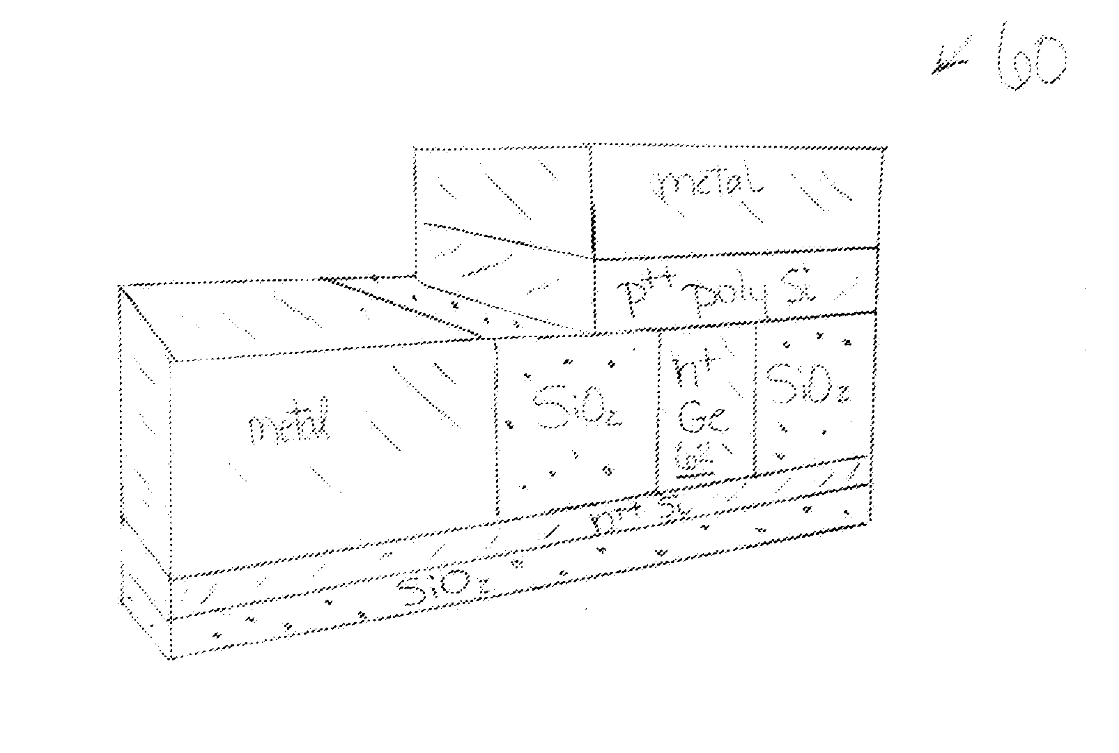
This patent describes a method and device for improving the efficiency of photonic devices. The device includes two silicon electrodes separated by a layer of germanium. The germanium layer contains additional dopant atoms to create an electrically-pumped guided mode as a laser gain medium. This increases the laser's efficiency and helps to overcome electrical losses in the device. The method involves forming the first silicon electrode, adding n-type dopant atoms to the germanium layer to create a background electrical dopant concentration, and then adding additional dopant to support the electrically-pumped guided mode. This device and method have improved performance compared to traditional photonic devices.

Problems solved by technology

Generally, defects in a semiconducting material, e.g., damage that is generated by the doping process itself, can limit the activation of dopants.
But the temperature that is required for a very high degree of dopant activation by annealing is for many applications too aggressive for integration into advanced semiconductor fabrication sequences with nanometric device features.
As a result, it is found that for many semiconducting materials, there is some limit of activated dopant concentration beyond which most conventional doping processes fail.
For example, ion implantation enables full control of dopant location, including directionality, but for many materials causes severe lattice damage that in general results in a low fraction of activated dopant even when high a high concentration of dopant is physically present.
Solid phase diffusion is limited by the diffusivity characteristics of a given semiconductor material, and vapor-phase diffusion processes typically require a temperature that cannot be tolerated in nano-scale device fabrication with many materials.
For a wide range of important semiconducting materials, high-concentration active doping has therefore remained difficult, and is in general impossible in the context of conventional high-throughput silicon-based fabrication processes and equipment.

Method used


Image

  • High-Concentration Active Doping in Semiconductors and Semiconductor Devices Produced by Such Doping
  • High-Concentration Active Doping in Semiconductors and Semiconductor Devices Produced by Such Doping
  • High-Concentration Active Doping in Semiconductors and Semiconductor Devices Produced by Such Doping

Examples


example 1

Ge In Situ Doping and Ex Situ Doping with Delta Dopant Layers

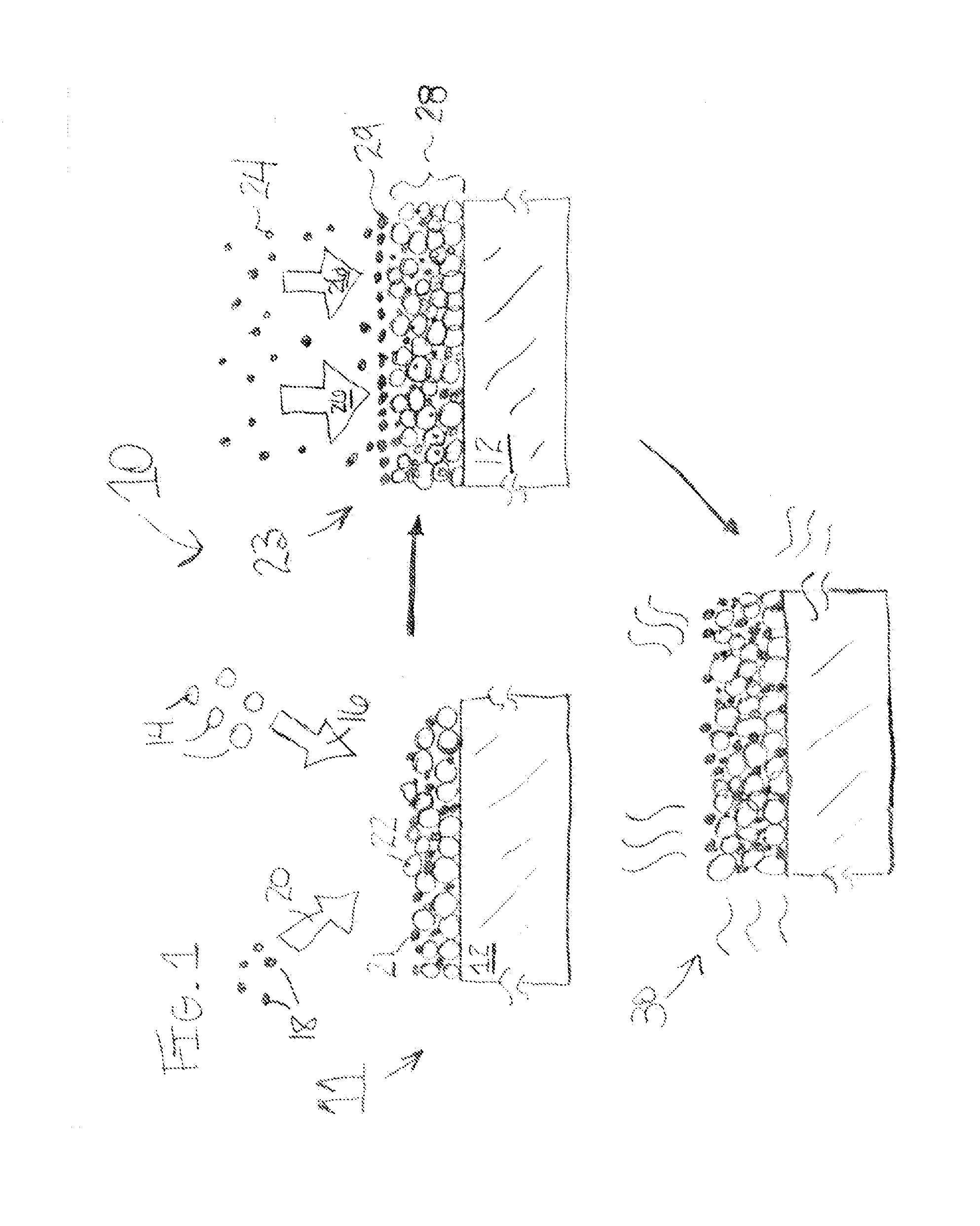
[0094]Ge layers were epitaxially grown on 6″ Si (100) substrates using a hot-wall UHVCVD reactor. A 30 nm-thick Ge buffer layer was first directly grown on the Si substrates at a temperature of 360° C. Then a 300 nm-thick Ge layer with in situ doping of phosphorous at a doping level of 1×1019 cm−3 was grown at an elevated temperature of 650° C. with gas flow of 3.8 sccm of GeH4 and 12 sccm PH3. For comparison, there was also grown a 300 nm-thick Ge layer that was not in situ-doped during the Ge growth.

[0095]The substrates were then exposed to PH3 gas flow of 12 sccm at 400° C. for 5 min to deposit a layer of P atoms onto the Ge surface while at the same time desorbing hydrogen. Subsequently, a 60 nm-thick intrinsic Ge layer was deposited at 400° C. Several cycles of PH3 saturation and intrinsic Ge growth were performed in the reactor to encapsulate multiple layers of P dopant atoms. For several samples, four encapsulated d...

example 2

Ge In Situ Doping and Ex Situ Doping by Ion Implantation

[0106]Ge layers were epitaxially grown on 6″ Si (100) substrates using a hot-wall UHVCVD reactor. A 30 nm-thick Ge buffer layer was first directly grown on the Si substrates at a temperature of 360° C. Then a 500 nm-thick Ge layer with in situ-doped phosphorous at a doping level of 1×1019 cm−3 was grown at an elevated temperature of 650° C. with a 3.8 sccm GeH4 gas flow and a 12 sccm PH3 gas flow.

[0107]After active layer growth, three different ion implantation processes were conducted, as given in Table I below.

TABLE 1TiltEnergyDoseEnergyDose#angle °ions(keV)(cm−2)ions(keV)(cm−2)17P1007.3 × 1015———27P1003.5 × 1015As2503.8 × 101537P1003.5 × 1015Sb3754.1 × 1015

[0108]After implantation, the samples were annealed to diffuse the implanted ions into the Ge active layer. RTA processes having a temperature of 600° C.-800° C., and durations of 30 s-180 s were conducted.

[0109]FIG. 13 is a plot of measured photoluminescence intensity as ...

example 3

Ge Laser Fabrication and Operation

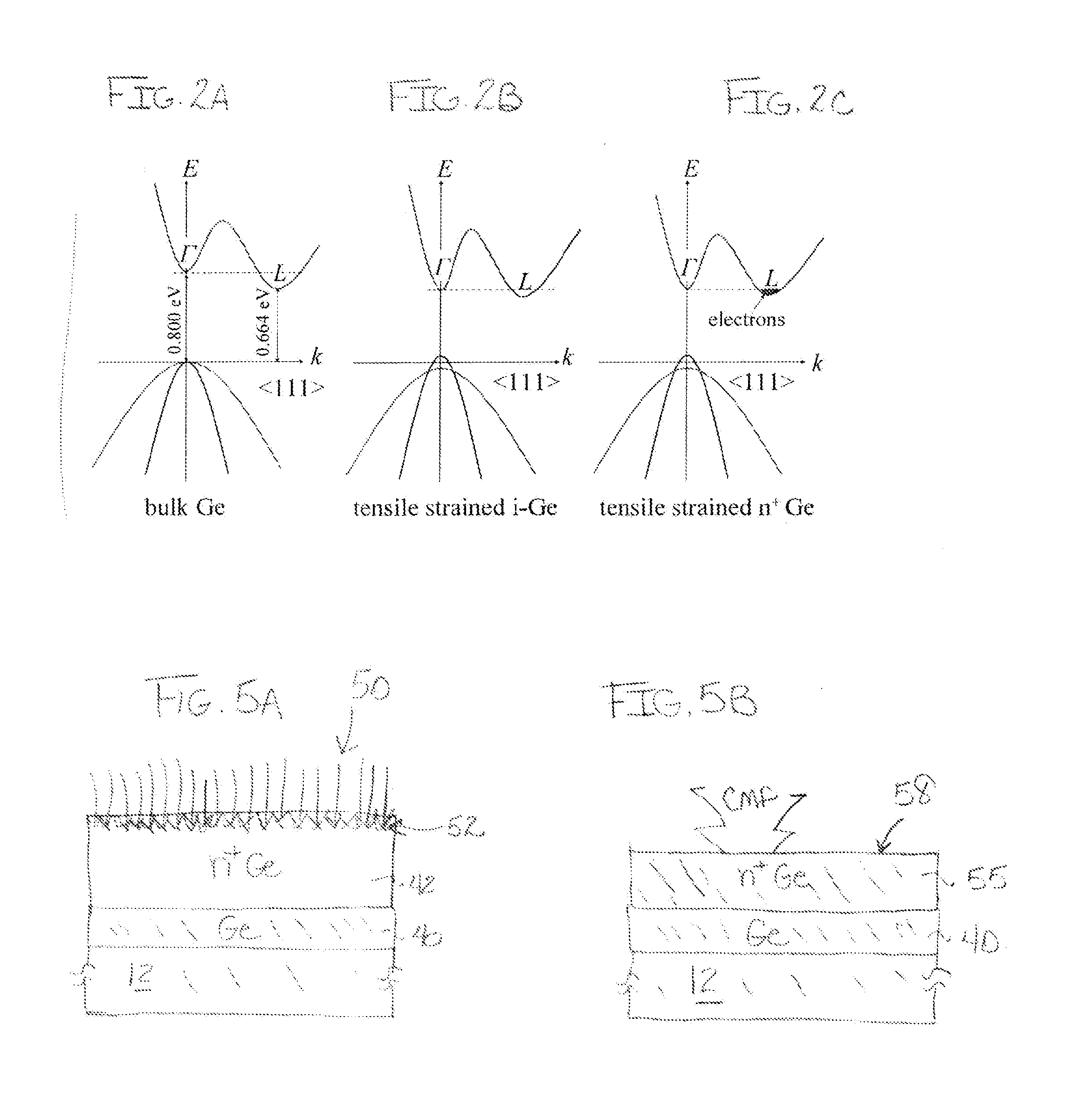
[0112]A vertical-injection, electrically-pumped Ge laser was fabricated in the manner of the fabrication sequence of FIGS. 7A-7K described above, employing the process of Example 1 above for producing a Ge buffer layer of 30 nm in thickness and Ge active layer of about 300 nm, doped in situ with phosphorus doping of 1×1019 cm−3, here conducted as mesa growth in a trench window in a silicon dioxide layer as in FIG. 7D. Four encapsulated phosphorus delta layers were formed, with a silicon dioxide capping layer of 100 nm in thickness to prevent out diffusion. Thermal annealing for diffusion of phosphorus from the delta doped layers into the Ge active layer was conducted by RTA at 700° C. for 1 minute. Then the structure was then planarized, as in FIG. 7F, by CMP, to remove the delta doping and capping layers from the active Ge layer surface. The remaining thickness of the Ge active layer after CMP as measured across the substrate and found to vary betw...


PUM


Abstract

In a method of forming a photonic device, a first silicon electrode is formed, and then a germanium active layer is formed on the first silicon electrode while including n-type dopant atoms in the germanium layer, during formation of the layer, to produce a background electrical dopant concentration that is greater than an intrinsic dopant concentration of germanium. A second silicon electrode is then formed on a surface of the germanium active layer. The formed germanium active layer is doped with additional dopant for supporting an electrically-pumped guided mode as a laser gain medium with an electrically-activated n-type electrical dopant concentration that is greater than the background dopant concentration to overcome electrical losses of the photonic device.

Description

CROSS-REFERENCE TO RELATED APPLICATIONS[0001]This application claims the benefit of U.S. Provisional Application No. 61 / 495,455, filed Jun. 10, 2011, the entirety of which is hereby incorporated by reference.STATEMENT REGARDING FEDERALLY SPONSORED RESEARCH[0002]This invention was made with Government support under Contract No. N00421-03-9-002, awarded by the Naval Air Warfare Center-Aircraft Division, and under Contract No. FA9550-06-1-0470, awarded by the Air Force Office of Scientific Research. The Government has certain rights in the invention.BACKGROUND[0003]This invention relates generally to techniques for electrically doping semiconducting materials, and more particularly relates to high-concentration doping of semiconducting materials in the fabrication of semiconductor devices.[0004]High-concentration electrical doping of semiconducting materials is becoming increasingly important for enabling advanced-performance electronic and optoelectronic devices. Conventionally, one o...

Claims


Application Information

Patent Timeline
Patent Type & Authority Applications(United States)
IPC IPC(8): H01S5/30H01S5/227
CPCH01S5/3086H01S5/3027H01S5/227H01L21/0237H01L21/0245H01L21/02532H01L21/02576H01L21/0262H01L21/02661H01L21/02664H01L21/2254H01L21/26513H01S5/0421H01S5/0422H01S5/2214H01S5/3054H01S5/3223H01L21/225H01L21/2251
Inventor BESSETTE, JONATHAN T.CAI, YANCAMACHO-AGUILERA, RODOLFO E.LIU, JIFENGKIMERLING, LIONELMICHEL, JURGEN
Owner MASSACHUSETTS INST OF TECH
Learn More