
Planar light emitting device

a light-emitting device and planar technology, applied in the direction of thermoelectric device junction materials, semiconductor devices, electrical equipment, etc., can solve the problems of low light-emitting efficiency, low light-emitting efficiency, and low light-emitting efficiency, so as to improve light-emitting efficiency and reduce total reflection loss , the effect of improving the light-emitting efficiency

Inactive Publication Date: 2014-08-14
PANASONIC CORP
View PDF4 Cites 12 Cited by
  • Summary
  • Abstract
  • Description
  • Claims
  • Application Information

AI Technical Summary

Benefits of technology

The present invention is aimed at proposing a planar light emitting device that can reduce total reflection loss, improve light outcoupling efficiency, and have excellent water and weather resistance.

Problems solved by technology

Consequently, it is expected that improvement of these two factors (electrical-optical conversion) are not so effective for an increase in the efficiency of the organic EL element.
This light outcoupling efficiency is not high.
Such low light outcoupling efficiency means 70 to 80% of the total amount of emitted light does not effectively contribute to light emission.
Unfortunately, the total reflection at the interface between the organic layer and the glass layer tends to cause a great loss.
With regard to the effort (1), available material is limited, and some of available material may cause great decreases in the light emission efficiency and lifetime.
It is therefore now difficult to improve the light outcoupling efficiency in line with this effort (1).
However, the high refractive index glass is much more expensive than generally-used glass, and the high refractive index glass is impractical in view of the industrial availability.
Thus, many of the high refractive index glass are fragile and have insufficient weatherproof properties.
Further, the surface of the plastic substrate easily suffers from scratches.
Therefore, the weather resistance seems to be insufficient.
However, the structure disclosed by this document does not have sufficient weather resistance.
Further, the structure becomes complex and the production process becomes troublesome, and thus this structure has a disadvantage in the production cost thereof.
However, this structure requires additional parts to make connection with electrodes.
Hence, the structure becomes more complex and the production process becomes more troublesome.
Further, the above structure is devoid of the light outcoupling structure, and therefore the sufficient improvement of the light outcoupling efficiency is not expected.

Method used


Image

  • Planar light emitting device
  • Planar light emitting device
  • Planar light emitting device

Examples


first embodiment

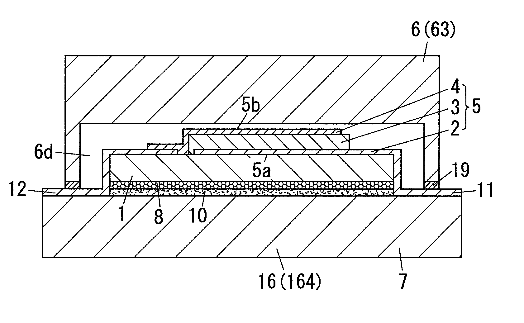
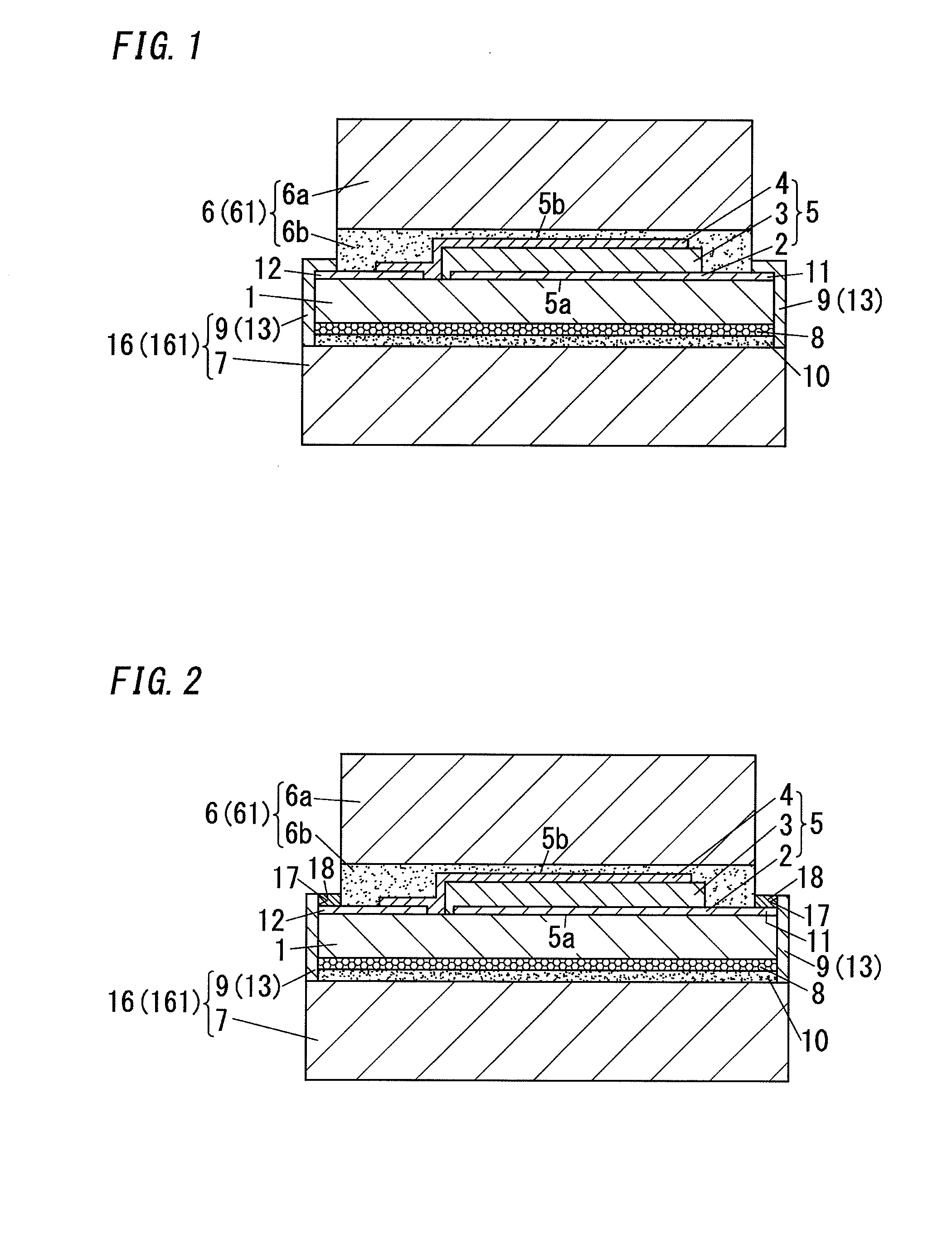
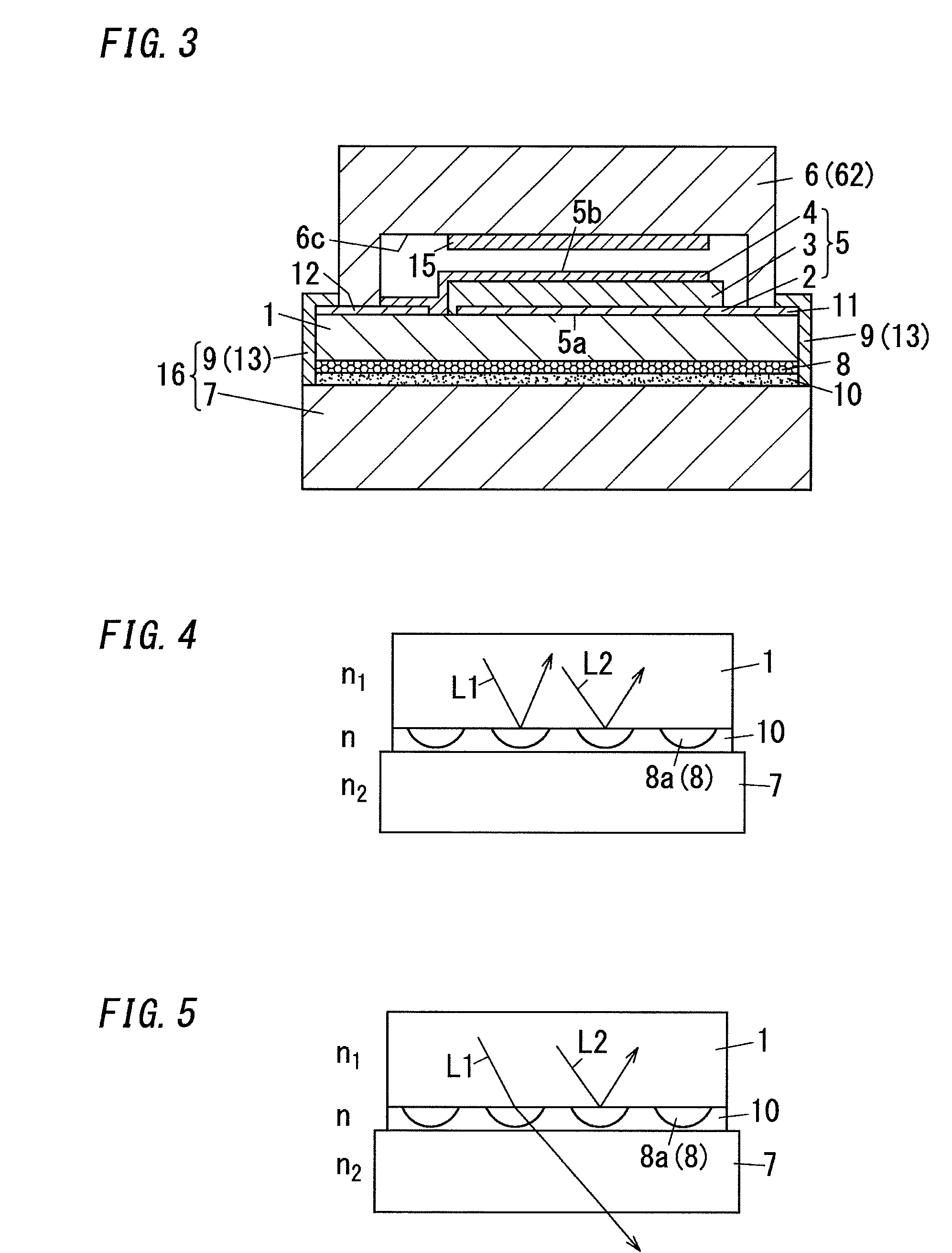
[0048]FIG. 1 shows an example of a planar light emitting device of the first embodiment. In this planar light emitting device, an organic electroluminescence element 5 (organic EL element 5) is formed on a surface of a formation substrate 1 with a light transmissive property. The organic electroluminescence element 5 includes a first electrode 2, a light emitting layer 3, and a second electrode 4 which are arranged in this order from the formation substrate 1. The first electrode 2 has a light transmissive property.

[0049]In other words, the planar light emitting device of the present embodiment includes an organic EL element 5 and a formation substrate 1. The organic EL element 5 includes a first surface (lower surface in FIG. 1) 5a and a second surface (upper surface in FIG. 1) 5b which are opposite surfaces in a thickness direction (upward and downward direction in FIG. 1) thereof. The organic EL element 5 is configured to emit light via the first surface 5a. The formation substra...

examples

[0179]Hereinafter, examples of manufacture of the planar light emitting device including the organic EL element are described.

[0180](Formation Substrate, Light Outcoupling Layer, Protection Substrate)

[0181]A PET substrate was used as the formation substrate 1 of the organic EL element. The PET substrate has refractive index higher than normal glass and is of a typical plastic material. A prism sheet with an adhesive was attached to a light exit surface of this substrate (opposite surface of the substrate from the light emitting layer 3). The prism sheet was dried in vacuum in advance. The prism sheet is a light diffusion film (available from KIMOTO; product name: LIGHT-UP (registered trademark) GM3). This light diffusion film is a sheet provided at its surface with the recessed and protruded structure 8a.

[0182]The protection substrate 7 prevents moisture from reaching the organic EL element 5 and has a light transmissive property. Hence, a glass substrate was used as the protection...

second embodiment

[0209]FIG. 8 shows an example of the planar light emitting device of the second embodiment. Like the embodiment shown in FIG. 1, in the present planar light emitting device, the organic EL element 5 is formed on the surface of the formation substrate 1 with a light transmissive property. The organic EL element 5 includes the first electrode 2, the light emitting layer 3, and the second electrode 4 which are arranged in this order from the formation substrate 1. The first electrode 2 has a light transmissive property. Further, like the embodiment shown in FIG. 1, the first protector 6 (61), the protection substrate 7, the light outcoupling structure 8, and the bonding layer 10 are provided. In the present embodiment, the second protector 9 has the inside block structure. For example, the second protector 9 is a gas barrier layer 14 formed on the surface of the formation substrate 1 close to the organic EL element 5. The other configurations of the planar light emitting device of the ...


PUM


Abstract

The planar light emitting device according to the present invention includes: an organic electroluminescence element; a formation substrate of a light transmissive resin material being adjacent to a first surface of the organic electroluminescence element; a light outcoupling structure provided to the formation substrate and suppressing reflection of light emitted from the organic electroluminescence element at a surface of the formation substrate; a first moisture preventer with a moisture proof property being over a second surface of the organic electroluminescence element to cover the organic electroluminescence element; and a second moisture preventer with a moisture proof property covering the formation substrate to prevent moisture from passing through the formation substrate and reaching the first surface of the organic electroluminescence element. The second moisture preventer includes an overlap overlapping the first surface in the thickness direction of the organic electroluminescence element. The overlap is of a light transmissive material.

Description

TECHNICAL FIELD[0001]The present invention relates to planar light emitting devices and particularly to a planar light emitting device with an organic electroluminescence element.BACKGROUND ART[0002]In a known general structure of an organic electroluminescence element (hereinafter referred to as “organic EL element”), a transparent electrode used as an anode, a hole transport layer, a light emitting layer, an electron injection layer, and a cathode are stacked on a surface of a transparent substrate in this order. It is known that such an organic EL element is used to produce a planar light emitting device (lighting panel). In this organic EL element, light is produced in an organic light emitting layer in response to application of voltage between the anode and the cathode, and the produced light is emitted outside through the transparent electrode and the transparent substrate and goes outside.[0003]The organic EL element gives a self-emission light in various wavelengths, with a...

Claims


Application Information

Patent Timeline
Patent Type & Authority Applications(United States)
IPC IPC(8): H01L51/52
CPCH01L51/524H01L51/5275H01L51/5259H10K59/871H10K59/879H10K59/874H10K50/858H10K50/841H10K50/846
Inventor YAMAE, KAZUYUKIHAYASHI, SHINTARO
Owner PANASONIC CORP
Learn More