
Systems and methods for error detection and correction in a memory module which includes a memory buffer

a memory module and error detection technology, applied in the direction of instruments, coding, code conversion, etc., can solve the problems of data stored in memory storage devices that may be subjected to electronic, corrupted or changed, and capabilities typically require a considerable amount of overhead

Active Publication Date: 2014-07-31
RAMBUS INC
View PDF22 Cites 3 Cited by
  • Summary
  • Abstract
  • Description
  • Claims
  • Application Information

AI Technical Summary

Benefits of technology

This solution enhances memory system reliability by enabling the use of more error-prone memory storage devices without compromising system integrity, reducing the need for extensive changes to host controllers and infrastructure, and mitigating the complexity of multi-error detection and correction processes.

Problems solved by technology

Data stored in memory storage devices may be subjected to electronic, electromagnetic or other forms of interference that can corrupt or change the stored value.
However, these capabilities typically require a considerable amount of overhead, in terms of access latency and the calculation and storage of parity bits, for example.
Host memory controllers designed to support error correction for low latency applications typically limit the error correction capability to the detection and correction of a “single error”, and the detection of two or more errors within a data word.
A “single error” may be in the form of a single bit, or in certain cases, the failure of a single memory device that results in the failure of multiple bits in adjacent locations within a data word.
Host controllers of this sort typically do not support the correction of “multi-errors”—i.e., errors in the form of multiple bits or the failure of multiple memory devices - assuming that the memory storage devices are highly reliable and that storage errors occur only as a result of low probability interference that corrupts the values stored in the memory device.
One trend in the development of memory storage devices is that as the storage cells continue to shrink due to advancements in process technology, the storage cells may be more susceptible to interference that corrupts the stored values.
Consequently, multi-errors within a single data word may occur with higher degrees of probability in future memory systems.
However, conventional methods of correcting such errors typically require significant changes to the host controller and the system infrastructure, and negatively impact the storage overhead and access latency characteristics of the memory system.

Method used


Image

  • Systems and methods for error detection and correction in a memory module which includes a memory buffer
  • Systems and methods for error detection and correction in a memory module which includes a memory buffer
  • Systems and methods for error detection and correction in a memory module which includes a memory buffer

Examples


Embodiment Construction

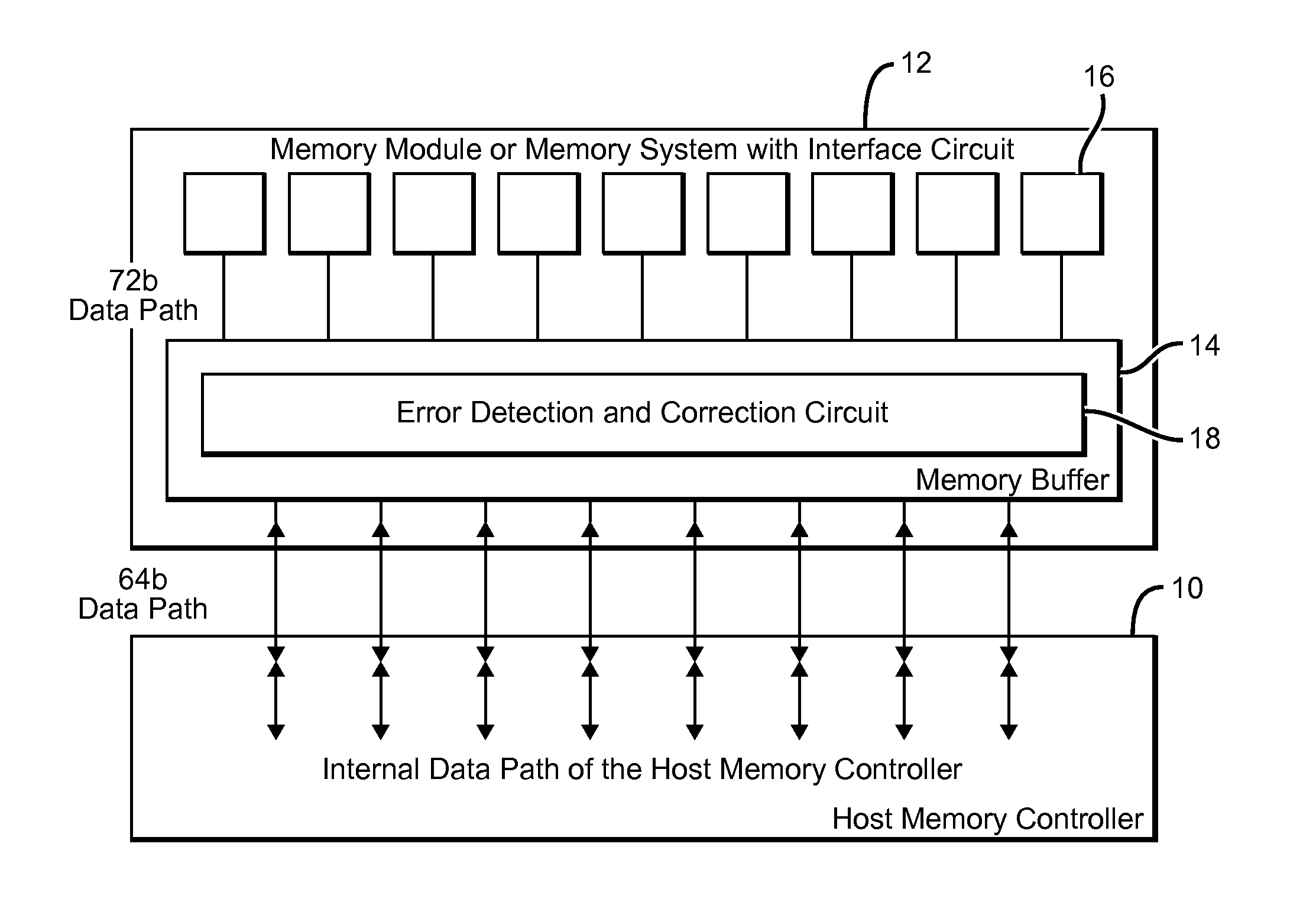
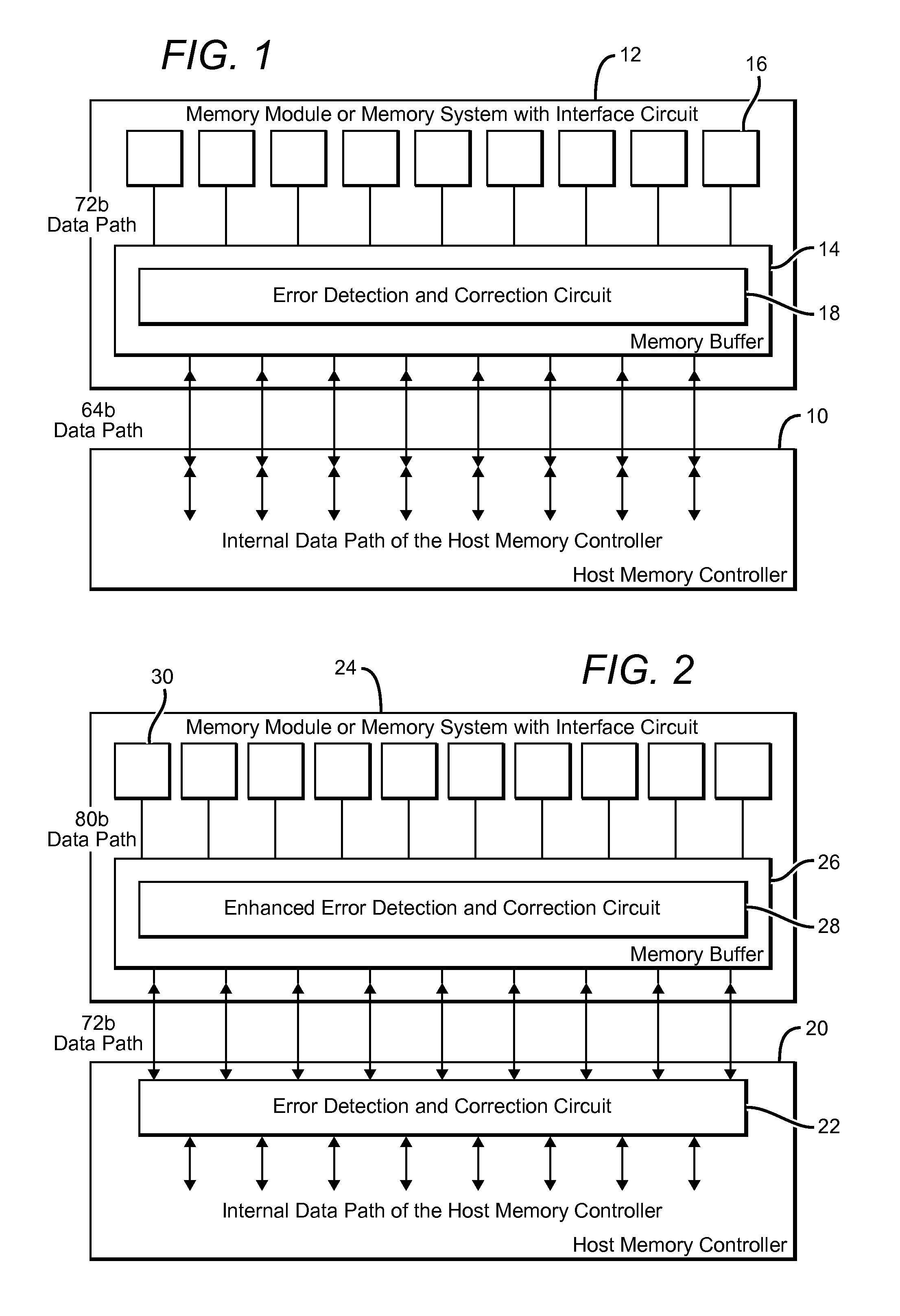
[0029]The present systems and methods are designed to improve memory system reliability for memory systems that do not detect or correct for data errors, as well as for systems that detect and correct for single errors and detect but do not correct multi-errors. The improvements in error correction capability enable computing systems without multi-error correction capability to utilize memory storage devices that are more susceptible to errors, without compromising the integrity requirements of the computing systems.

[0030]The systems and methods may be implemented in different ways for different systems. Multiple implementations are described herein as illustrative examples; the examples should not be construed as limiting the present invention in nature. Common to all systems to which the present system is applicable is a host controller which is coupled to an interface device that acts as an interface between the host controller and a plurality of RAM chips, and which includes an ...


PUM


Abstract

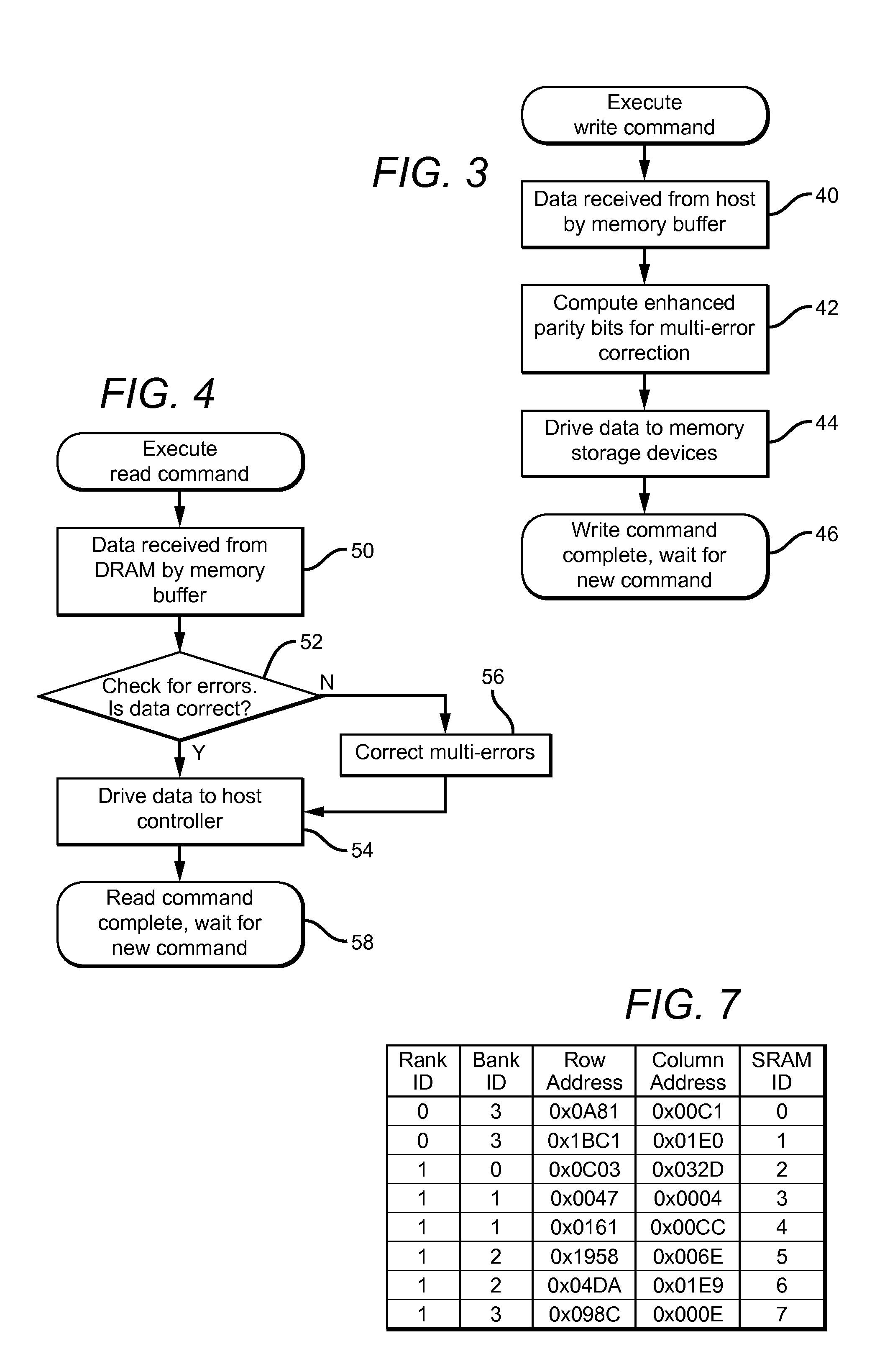
The present systems include a memory module containing a plurality of RAM chips, typically DRAM, and a memory buffer arranged to buffer data between the DRAM and a host controller. The memory buffer includes an error detection and correction circuit arranged to ensure the integrity of the stored data words. One way in which this may be accomplished is by computing parity bits for each data word and storing them in parallel with each data word. The error detection and correction circuit can be arranged to detect and correct single errors, or multi-errors if the host controller includes its own error detection and correction circuit. Alternatively, the locations of faulty storage cells can be determined and stored in an address match table, which is then used to control multiplexers that direct data around the faulty cells, to redundant DRAM chips in one embodiment or to embedded SRAM in another.

Description

RELATED APPLICATIONS[0001]This application is a Continuation of U.S. utility application Ser. No. 13 / 445,143, filed Apr. 12, 2012, still pending, which claimed the benefit of provisional patent application No. 61 / 475,184 to Wang et al., filed Apr. 13, 2011.BACKGROUND OF THE INVENTION[0002]1. Field of the Invention[0003]This invention relates generally to error detection and correction techniques for use with a memory module which includes a memory buffer that serves as an interface between a host controller and the RAM chips residing on the module.[0004]2. Description of the Related Art[0005]Data stored in memory storage devices may be subjected to electronic, electromagnetic or other forms of interference that can corrupt or change the stored value. Consequently, memory systems designed for reliable operation have been constructed with error detection and correction capabilities to detect and correct for errors that occur in the storage devices. However, these capabilities typicall...

Claims


Application Information

Patent Timeline
Patent Type & Authority Applications(United States)
IPC IPC(8): G06F11/10G11C29/52
CPCG06F11/10H03M13/1515H03M13/152G11C7/1006G11C11/408G11C29/848G11C2029/0411G06F11/1068G11C29/52
Inventor WANG, DAVIDHAYWOOD, CHRISTOPHER
Owner RAMBUS INC
Learn More