
Optical phased arrays

Active Publication Date: 2014-07-10
MASSACHUSETTS INST OF TECH
View PDF3 Cites 95 Cited by
  • Summary
  • Abstract
  • Description
  • Claims
  • Application Information

AI Technical Summary

Benefits of technology

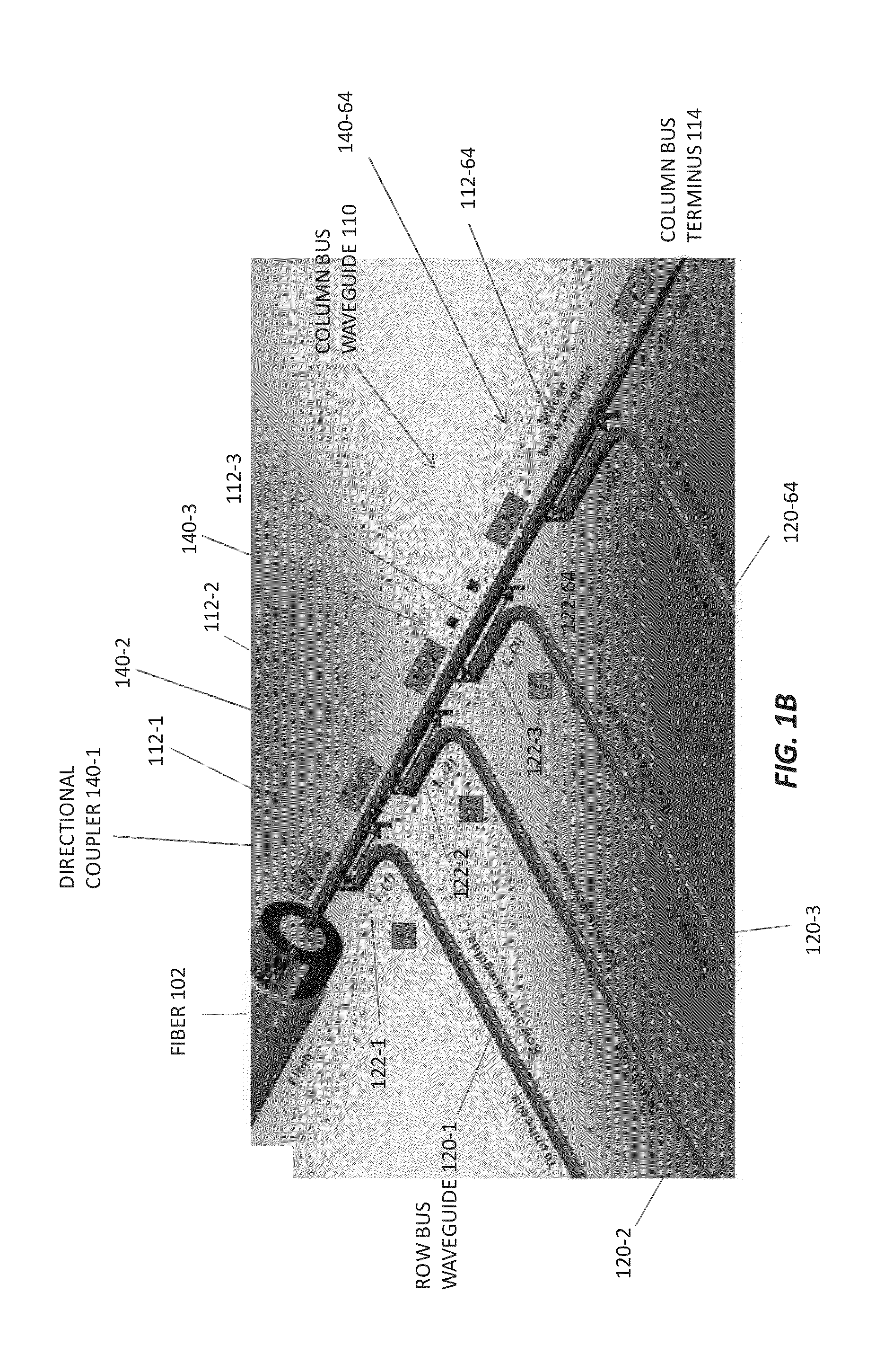
The present invention relates to an optical phased array for forming a far-field radiation pattern from a coherent optical beam. The optical phased array includes a column waveguide that guides the coherent optical beam to a plurality of antenna elements. The antenna elements emit the coherent optical beam to form the far-field radiation pattern. The optical phased array can be used in various applications such as optical communication systems and imaging devices. The technical effects of the invention include improved far-field radiation pattern, reduced resonant back-reflection, and compensation for phase errors.

Problems solved by technology

However, the short optical wavelength also imposes stringent requirements on fabrication.

Method used


Image

  • Optical phased arrays
  • Optical phased arrays
  • Optical phased arrays

Examples


Embodiment Construction

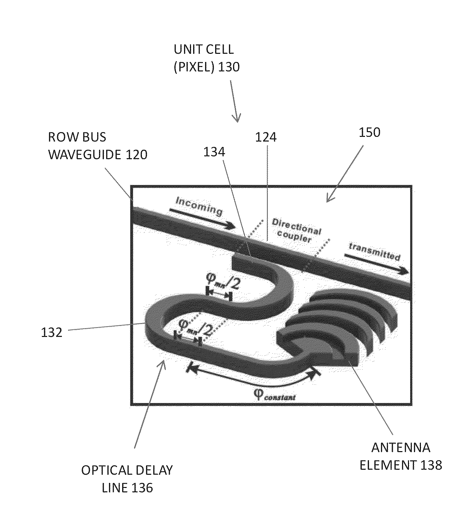
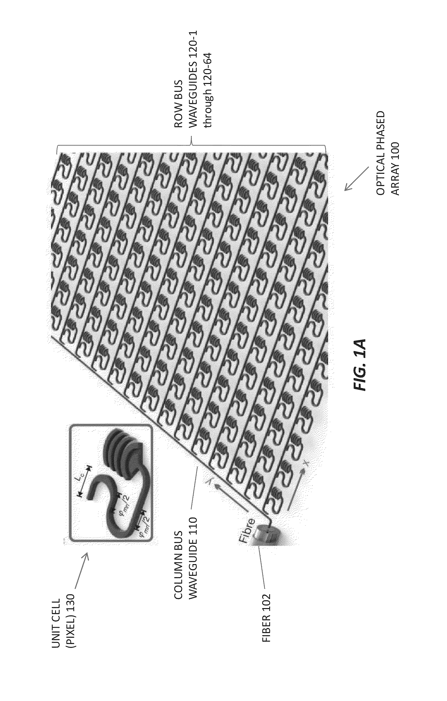
[0040]Examples of the present technology include a large-scale, two-dimensional optical phased array, also called a nanophotonic phased array (NPA), with optical nanoantennas that are densely integrated on a silicon chip within a relatively small footprint. For instance, an exemplary NPA may include 4,096 antenna elements arranged in a 64×64 element array in an area of about 576 μm×576 μm. The robust NPA designs disclosed herein, together with state-of-the-art complementary metal-oxide-semiconductor technology, allows large-scale NPAs to be implemented on compact and inexpensive nanophotonic chips.

[0041]An NPA, like its radio-frequency (rf) counterparts, comprises an array of optical antennas, also known as nanoantennas, nanophotonic antennas, antenna elements, or simply elements. For instance, an NPA may include a set of identical optical antennas arranged in a periodic, two-dimensional array with the elements separated by a distance on the order of an optical wavelength. In other ...


PUM


Abstract

An optical phased array formed of a large number of nanophotonic antenna elements can be used to project complex images into the far field. These nanophotonic phased arrays, including the nanophotonic antenna elements and waveguides, can be formed on a single chip of silicon using complementary metal-oxide-semiconductor (CMOS) processes. Directional couplers evanescently couple light from the waveguides to the nanophotonic antenna elements, which emit the light as beams with phases and amplitudes selected so that the emitted beams interfere in the far field to produce the desired pattern. In some cases, each antenna in the phased array may be optically coupled to a corresponding variable delay line, such as a thermo-optically tuned waveguide or a liquid-filled cell, which can be used to vary the phase of the antenna's output (and the resulting far-field interference pattern).

Description

CROSS-REFERENCE TO RELATED PATENT APPLICATION[0001]This application claims priority, under 35 U.S.C. §119(e), from U.S. Provisional Application 61 / 749,967, filed Jan. 8, 2013, entitled “Large-Scale Nanophotonic Phased Array,” which application is hereby incorporated herein by reference in its entirety.GOVERNMENT SUPPORT[0002]This invention was made with government support under Contract No. HR0011-12-2-0007 awarded by the Defense Advanced Research Projects Agency and under Grant No. DE-AC04-94AL85000 awarded by the Department of Energy. The government has certain rights in the invention.BACKGROUND[0003]Electromagnetic phased arrays at radio frequencies are well known and have enabled applications ranging from communications to radar, broadcasting and astronomy. The ability to generate arbitrary radiation patterns with large-scale phased arrays has long been pursued. Although it is extremely expensive and cumbersome to deploy large-scale radio frequency phased arrays, optical phased ...

Claims


Application Information

Patent Timeline
IPC IPC(8): G02F1/21G02F1/01
CPCG02B6/26G02F1/0147G02F1/218G02F1/2955G02B6/3546G02B6/3576G02B6/12033G02B6/29343
Inventor SUN, JIEWATTS, MICHAEL R.YAACOBI, AMITIMURDOGAN, ERMAN
Owner MASSACHUSETTS INST OF TECH
Learn More