Voltage-controlled magnetic anisotropy (VCMA) switch and magneto-electric memory (MERAM)
- Summary
- Abstract
- Description
- Claims
- Application Information
AI Technical Summary
Benefits of technology
Problems solved by technology
Method used
Image

Examples
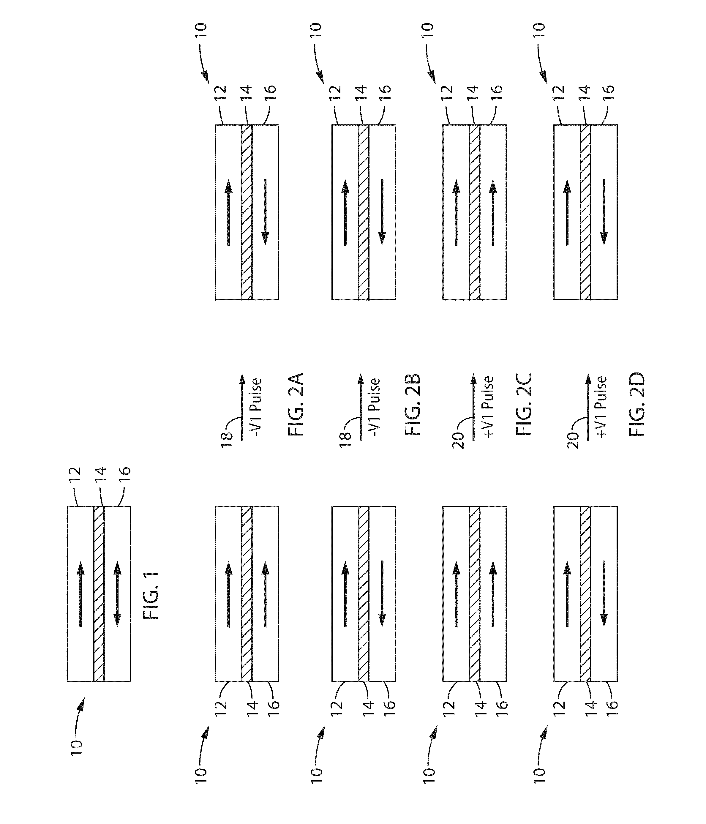
embodiment 10
[0046]FIG. 1 illustrates an in-plane VCMA switch embodiment 10, having the following layers, (metallic contacts are not shown). A ferromagnetic (FM) fixed layer 12, of ferromagnetic material, such as comprising Fe, Co, CoFe, or CoFeB. A ferromagnetic (FM) free layer 16, of ferromagnetic material, such as comprising Fe, Co, CoFe, or CoFeB. A dielectric (DE) tunnel barrier 14, of dielectric material, interposed between said FM free layer and FM fixed layer, such as comprising MgO. In the figure, the magnetic fields of the fixed and free layer are shown with opposite polarities. The overall structure resembles a magnetic tunnel junction (MTJ), and exhibits tunneling magnetoresistance (TMR) which allows for reading of the magnetic state of the FL by measuring the resistance across the stack, although the state of the switch is not current controlled.
[0047]It should be appreciated that each of the free and fixed layers may themselves comprise several sub-layers, that acting in combinatio...
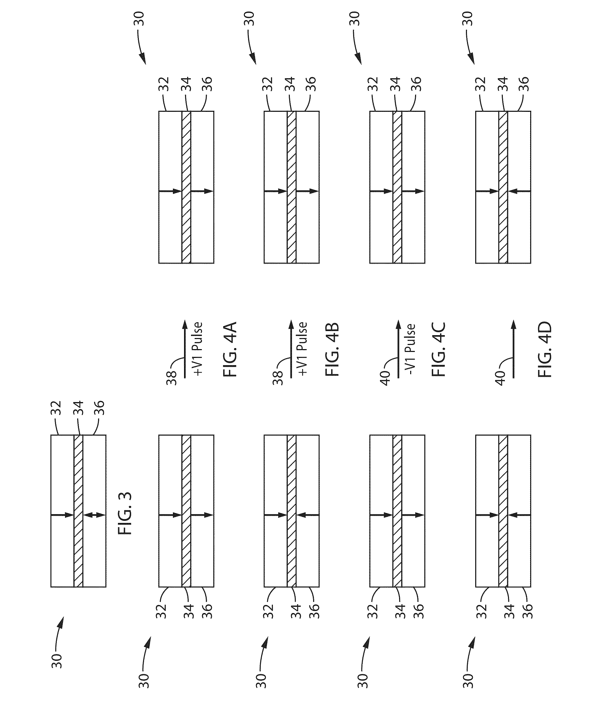
embodiment 30
[0064]FIG. 3 and FIG. 4A through FIG. 4D illustrate an OOP VCMA switch embodiment 30, having a fixed layer 32 (FM2) and free layer 36 (FM1) separated by a tunnel barrier 34. In this embodiment, the OOP anisotropy of the free layer is designed to be smaller than the OOP anisotropy of the fixed layer. For one polarity of the voltage (e.g., positive), the OOP anisotropy of the FL can be reduced, such that the FL magnetization turns into the sample plane, or is otherwise changed from the OOP state, for example by going to a nonuniform micromagnetic or domain state, or by starting a precessional motion around the effective magnetic field. Once this voltage is returned to zero, the magnetization returns to the OOP state, but the direction in which it will point is determined by the stray magnetic field from the fixed layer.
[0065]Positive voltages, as in −V1 pulse 38 in FIG. 4B, can therefore cause switching from anti-parallel (AP) to parallel (P) configuration, as seen by the arrows chang...
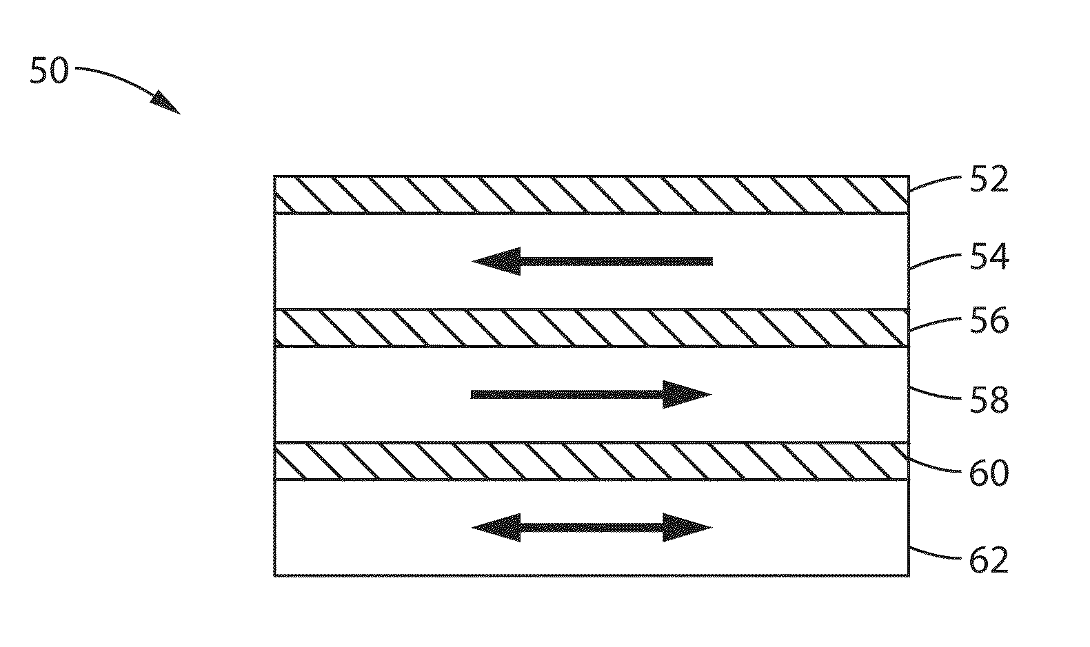
embodiment 50
[0080]FIG. 5, FIG. 6A through FIG. 6D, and FIG. 7A through FIG. 7D illustrate an embodiment 50 of an in-plane MeRAM bit, and its switching in two configurations. The MeRAM bit is shown comprising FM and DE layers of various compositions. It will be noted that the description does not describe the use of metal contact layers for the sake of simplicity, although one of ordinary skill in the art will appreciate the need of these contacts, such as on the two sides (top and bottom) of the entire layer stack.
[0081]In FIG. 5 the ferromagnetic layers are shown comprising a ferromagnetic semi-fixed layer 54 (FM3), a ferromagnetic fixed layer 58 (FM2), and a ferromagnetic free layer 62 (FM1). The MeRAM bit is shown comprising FM and DE layers of various compositions. The moniker of ‘semi-fixed’ layer is utilized because the magnetization for this layer can rotate for some applied voltages, but not for others. It will be noted that the description does not describe the use of metal contact lay...
PUM
 Abstract
Description
Claims
Application Information
 - R&D
- Intellectual Property
- Life Sciences
- Materials
- Tech Scout
- Unparalleled Data Quality
- Higher Quality Content
- 60% Fewer Hallucinations
Browse by: Latest US Patents, China's latest patents, Technical Efficacy Thesaurus, Application Domain, Technology Topic, Popular Technical Reports.
© 2025 PatSnap. All rights reserved.Legal|Privacy policy|Modern Slavery Act Transparency Statement|Sitemap|About US| Contact US: help@patsnap.com