Semiconductor structure and method for manufacturing the same

Active Publication Date: 2014-06-26
MACRONIX INT CO LTD
View PDF7 Cites 1 Cited by
  • Summary
  • Abstract
  • Description
  • Claims
  • Application Information

AI Technical Summary

Benefits of technology

The patent text describes a semiconductor structure and a method for manufacturing it. The structure has a stable breakdown voltage and is capable of withstanding higher gate voltage stress. The semiconductor structure includes a first doped region, a second doped region, and a gate structure. The gate structure comprises a first gate portion and a second gate portion separated by a gap. The technical effect of this structure is to provide a more reliable and efficient semiconductor structure for use in various electronic devices.

Problems solved by technology

The HTGB (high temperature gate bias) of a conventional 700V LDMOS device is about 20V, therefore, when a gate voltage of higher than 20V is applied to the device, the breakdown may decrease dramatically, causing the device failing to function.

Method used


Image

  • Semiconductor structure and method for manufacturing the same
  • Semiconductor structure and method for manufacturing the same
  • Semiconductor structure and method for manufacturing the same

Examples


Embodiment Construction

[0020]Preferred embodiments are disclosed below for elaborating the invention. The following embodiments are for the purpose of elaboration only, not for limiting the scope of protection of the invention. Besides, secondary elements are omitted in the following embodiments to highlight the technical features of the invention.

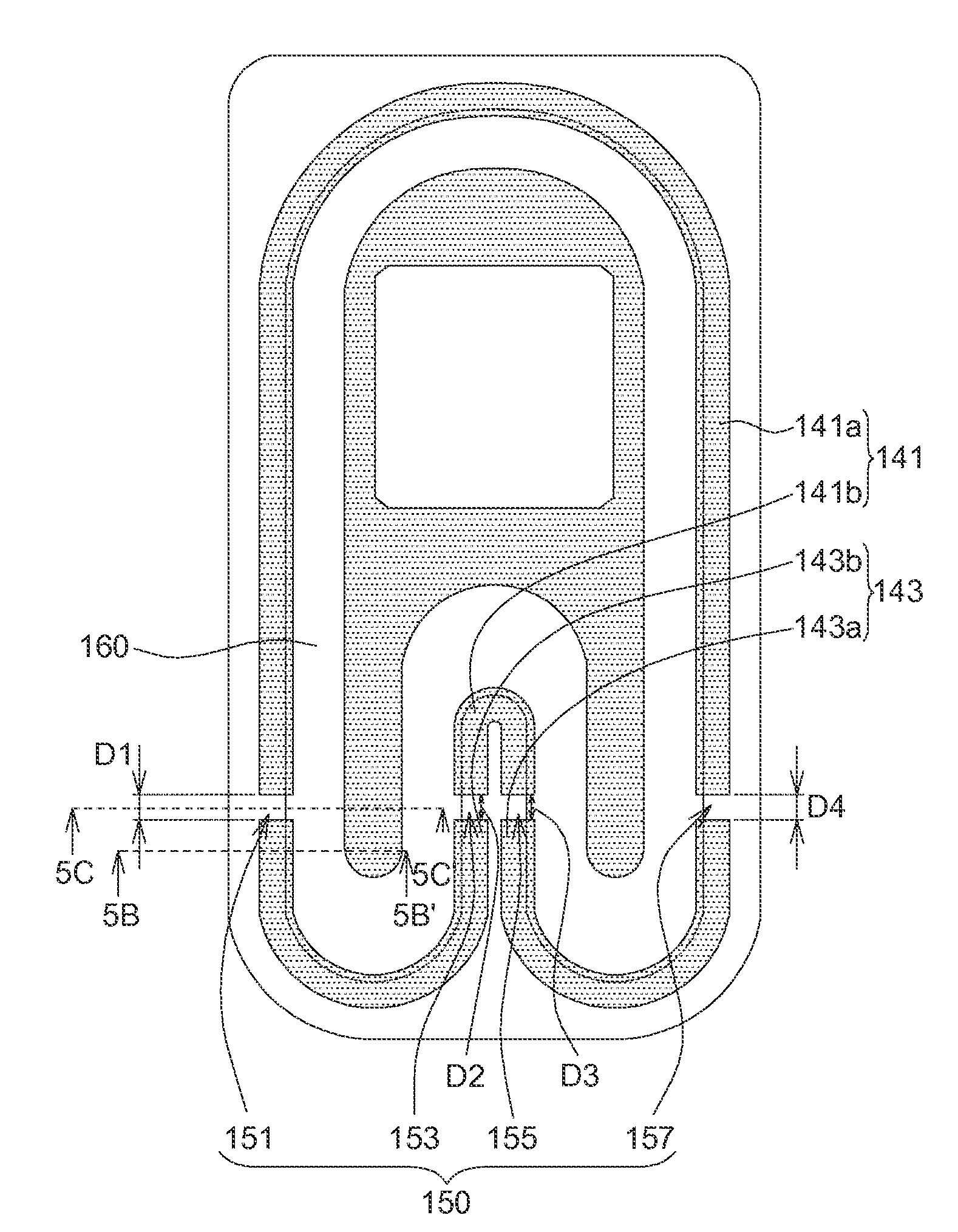
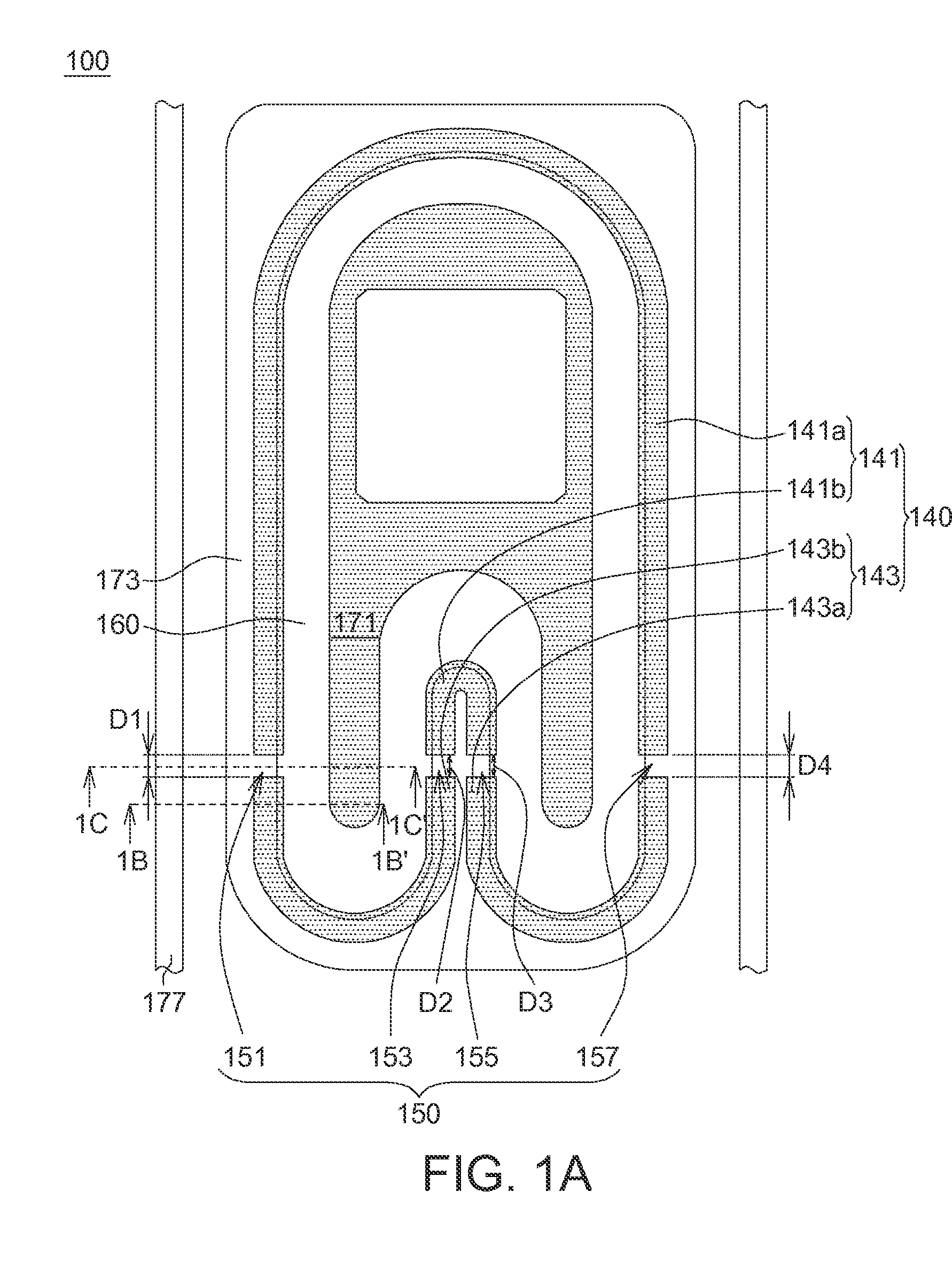
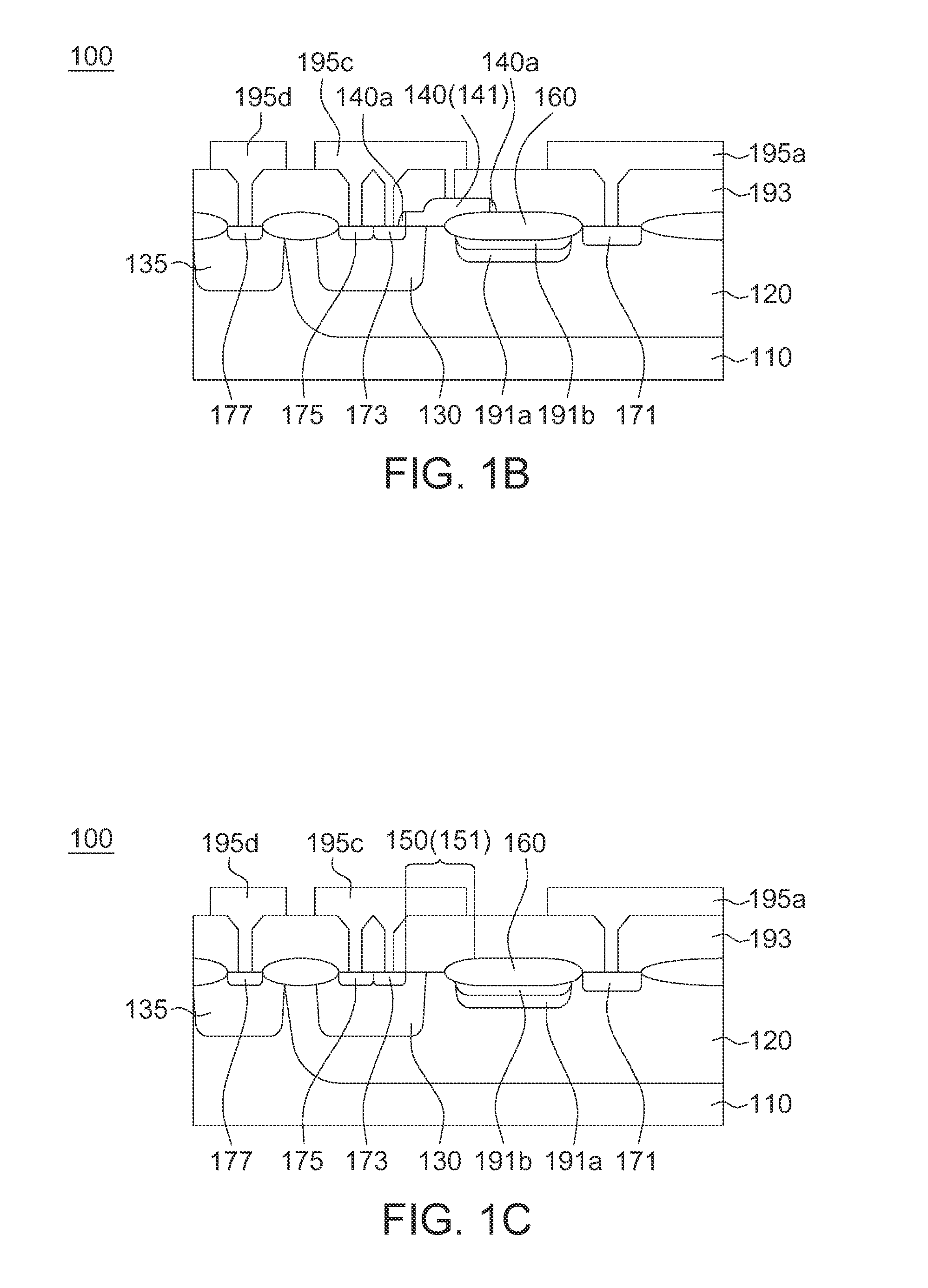
[0021]Referring to FIGS. 1A-1C, FIG. 1A shows a top view of a semiconductor according to an embodiment of the present disclosure, FIG. 1B shows a cross-sectional view along the section line 1B-1B′ in FIG. 1A, and FIG. 1C shows a cross-sectional view along the section line 1C-1C′ in FIG. 1A. The semiconductor structure 100 includes a first doped region 120, a second doped region 130, and a gate structure 140. The first doped region 120 has a first type conductivity. The second doped region 130 is formed in the first doped region 120 and has a second type conductivity opposite to the first type conductivity. The gate structure 140 is formed on the first doped regi...


PUM


Abstract

A semiconductor structure and a method for manufacturing the same are provided. The semiconductor structure comprises a first doped region, a second doped region, and a gate structure. The first doped region has a first type conductivity. The second doped region is formed in the first doped region and has a second type conductivity opposite to the first type conductivity. The gate structure is formed on the first doped region and the second doped region. The gate structure comprises a first gate portion and a second gate portion, which are separated from each other by a gap.

Description

BACKGROUND[0001]1. Technical Field[0002]The disclosure relates in general to a semiconductor structure and a manufacturing method thereof, and more particularly to a semiconductor structure, which can endure a relatively high gate voltage stress, and a manufacturing method thereof.[0003]2. Description of the Related Art[0004]A lateral diffused metal oxide semiconductor (LDMOS) device has its source and drain at the surface of the wafer causing a lateral current. Two important parameters in the design of LDMOS devices are breakdown voltage and on-state resistance. It is preferred to have a high breakdown voltage and a low on-state resistance to provide a device having relatively lower power consumption when operated under high voltage.[0005]The HTGB (high temperature gate bias) of a conventional 700V LDMOS device is about 20V, therefore, when a gate voltage of higher than 20V is applied to the device, the breakdown may decrease dramatically, causing the device failing to function. Th...

Claims


Application Information

Patent Timeline
IPC IPC(8): H01L27/088H01L21/02
CPCH01L29/7816H01L29/402H01L29/42368H01L29/4238H01L29/66689H01L29/0634H01L29/0692H01L29/0878H01L21/02697
Inventor CHAN, CHING-LINLIN, CHEN-YUANLIN, CHENG-CHILIEN, SHIH-CHIN
Owner MACRONIX INT CO LTD
Why Eureka
Try Eureka