
Normally off gallium nitride field effect transistors (FET)

a field effect transistor and gallium nitride technology, applied in the field of semiconductor device configuration and manufacturing methods, can solve the problems of more complicated devices, device not suitable for those applications, and additional power consumption, and achieve the effects of improving device configuration, simple and convenient manufacturing and operating processes, and improving device configuration

Active Publication Date: 2014-06-26
ALPHA & OMEGA SEMICON INC
View PDF2 Cites 7 Cited by
  • Summary
  • Abstract
  • Description
  • Claims
  • Application Information

AI Technical Summary

Benefits of technology

The present invention provides a new and improved device configuration and manufacturing method for a semiconductor GaN-based HFET power device. The device can be used as a normally-off device or a multiple-channel device. The device has a negative charged floating gate or a negative charged gate oxide layer to deplete the channel when no voltage is applied to the gate. The gate voltage is applied to offset the negative charge and restore the 2DEG channel formed on the hetero-junction between the layers. The device is simple and convenient to manufacture and operate, and solves the difficulties and limitations that previously existed.

Problems solved by technology

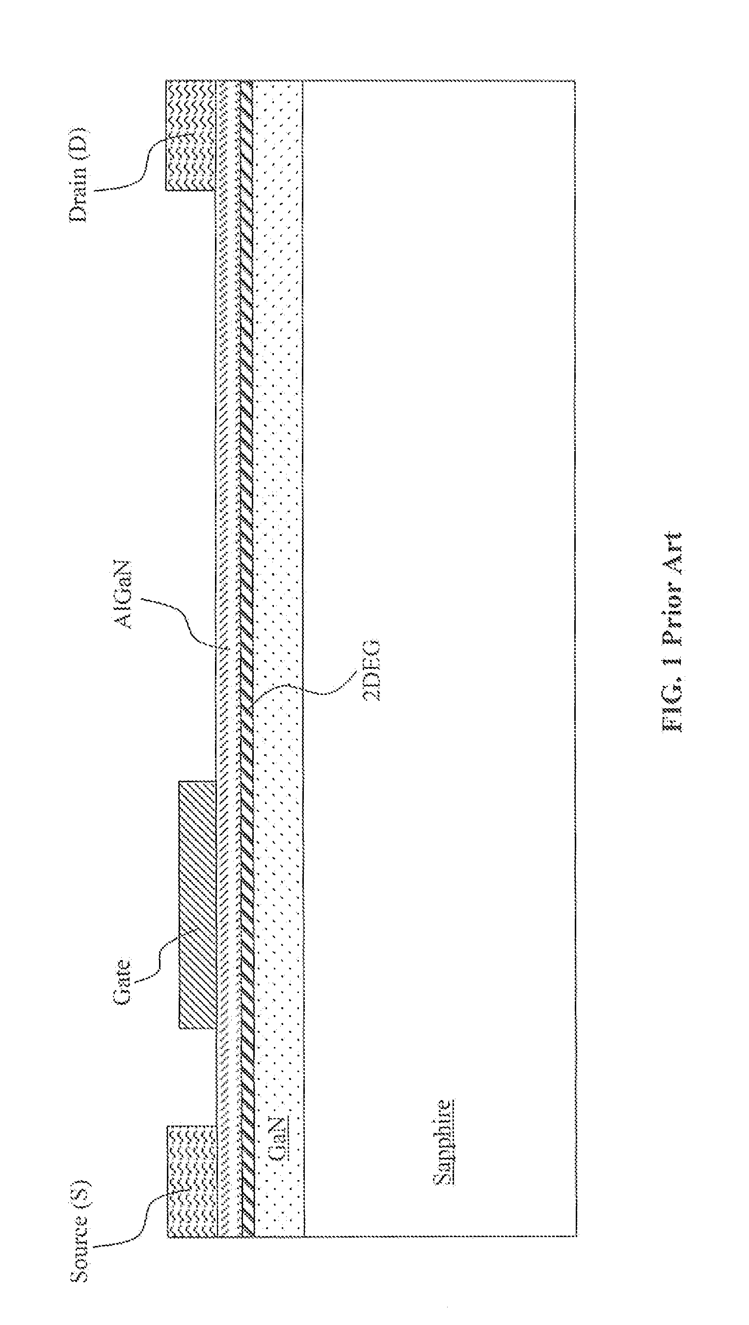
Conventional methods of configuring, and manufacturing a gallium nitride (GaN) based field effect transistors (FETs) are still continuously challenged with a technical issue for providing a normally-off FET transistor that has simple and convenient manufacturing and operating configurations.
A requirement to continuous apply a pinch off voltage to the gate in order to turn off the transistor thus leads to additional power consumptions and may often cause a more complicated device control process for implementing such transistor in an electronic device.
In addition most applications are designed for normally-off transistors and so this device would not be suitable to those applications.
But these types of transistors cannot be driven by a gate voltage between the traditional gate voltage of ten to fifteen volts.
However, such devices suffer the disadvantages of low inversion mobility and a very high electric field in the oxide when the device is biased into the breakdown thus causing device reliability concerns.
In order to address this issue, an oxide layer with increased thickness had been implemented, but that degraded the transconductance and lead to an undesirable higher RdsA.

Method used


Image

  • Normally off gallium nitride field effect transistors (FET)
  • Normally off gallium nitride field effect transistors (FET)
  • Normally off gallium nitride field effect transistors (FET)

Examples


Embodiment Construction

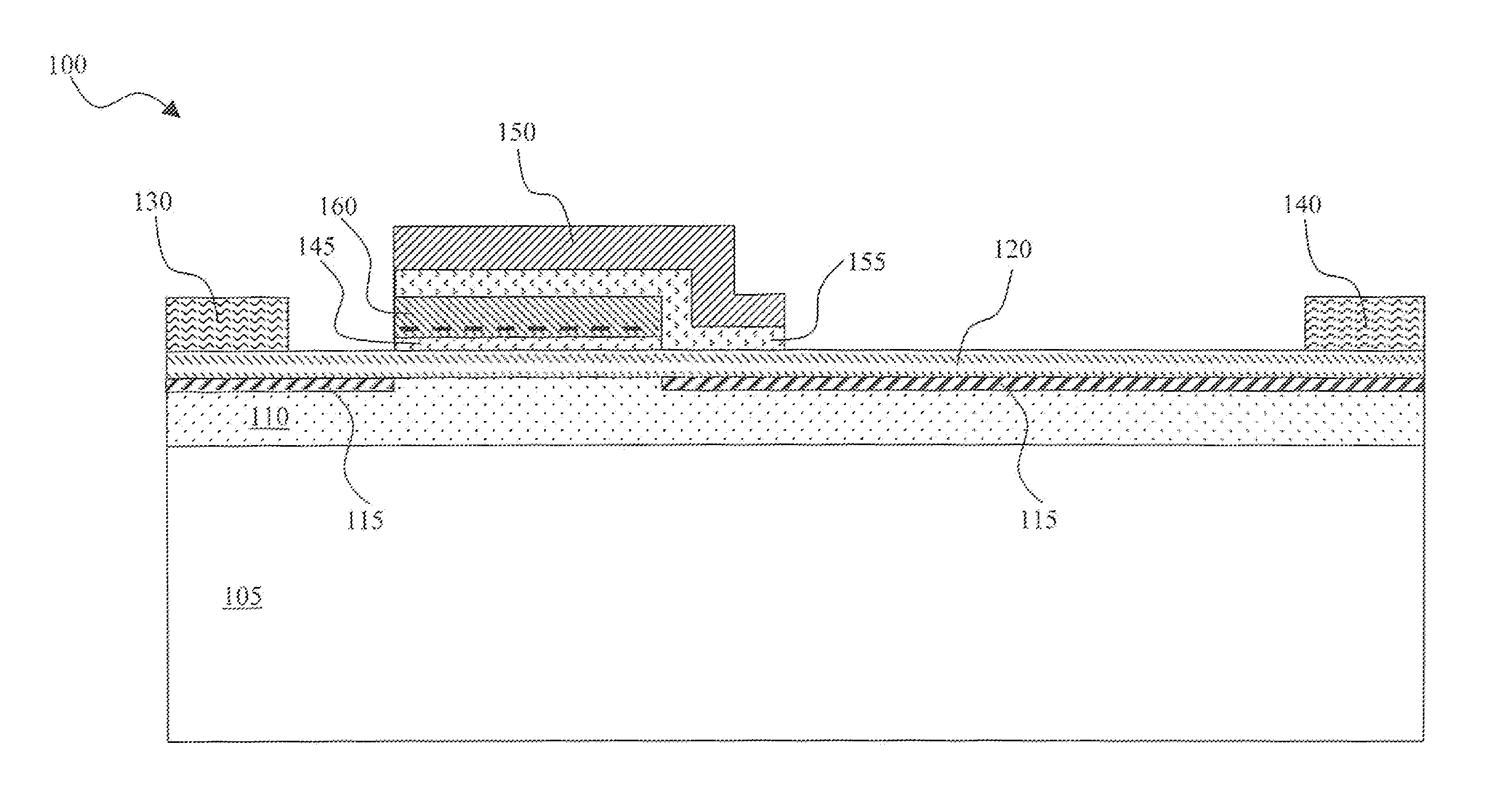
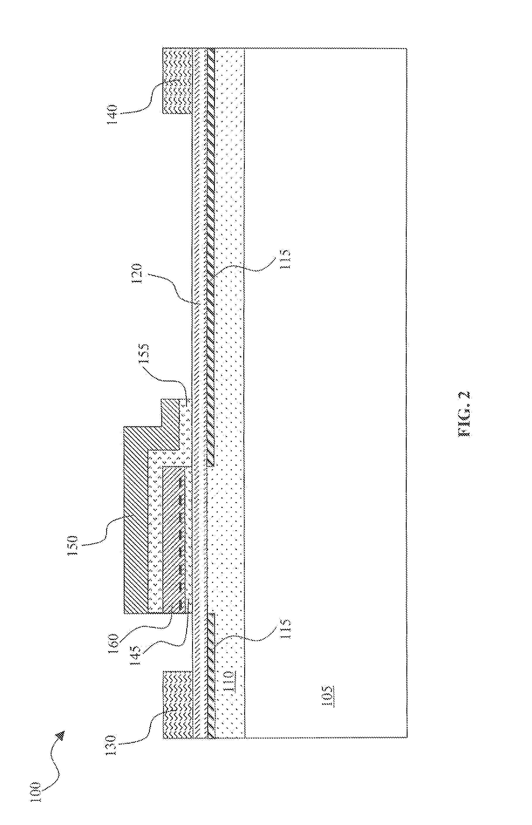
[0022]Referring to FIG. 2 for a cross sectional view of a heterostructure field effect transistor (HFET) semiconductor power device 100 of this invention. The HEFT semiconductor power device 100 comprises an AlGaN layer 120 epitaxial grown on top of gallium nitride (GaN) layer 110 thus forming a AlGaN / GaN hetero-junction with a two-dimensional electron gas (2DEG) 115 located at the interface. The AlGalN / GaN hetero-junction structure is supported on a sapphire substrate 105. A source electrode 130 and a drain 140 are disposed on two opposite sides of a gate electrode 150 to control the current flow through the 2DEG layer 115. The gate electrode 150 is insulated from the N-doped AlGaN layer 120 with a thicker gate oxide layer 155. In order to configure the HFET power device as a normally off device, a floating gate 160 is formed beneath at least a portion of the gate oxide layer 155. The floating gate 160 is insulated from the AlGaN layer 120 with a thin oxide layer 145, and from the ...


PUM


Abstract

A heterostructure field effect transistor (HFET) gallium nitride (GaN) semiconductor power device comprises a hetero-junction structure comprises a first semiconductor layer interfacing it second semiconductor layer of two different band gaps thus generating an interface layer as a two-dimensional electron gas (2DEG) layer. The power device further comprises a source electrode and a drain electrode disposed on two opposite sides of a gate electrode disposed on top of the hetero-junction structure for controlling a current flow between the source and drain electrodes in the 2DEG layer. The power device further includes a floating gate located between the gate electrode an hetero-junction structure, wherein the gate electrode is insulated from the floating gate with an insulation layer and wherein the floating gate is disposed above and padded with a thin insulation layer from the hetero-junction structure and wherein the floating gate is charged for continuously applying a voltage to the 2DEG layer to pinch off the current flowing in the 2DEG layer between the source and drain electrodes whereby the HFET semiconductor power device is a normally off device.

Description

[0001]This application is a Continuous Application, and claims priority of a pending application Ser. No. 12 / 589,945 filed on Oct. 30, 2009 by the common inventors of this Application. The benefit of the filing dates are hereby claimed under Title 35 of the United States Code. The disclosures of applications Ser. No. 12 / 589,945 are hereby incorporated by reference,BACKGROUND OF THE INVENTION [0002]1. Field of the Invention[0003]The invention relates generally to the configurations and methods of manufacturing the semiconductor devices. More particularly, this invention relates to a gallium nitride (GaN)-based field effect transistor implemented with new device configurations and manufacturing methods for a normally-off GaN-based field effect transistor that has an extremely small ON resistance in conducting a large amount of electric current.[0004]2. Description of the Prior Art[0005]Conventional methods of configuring, and manufacturing a gallium nitride (GaN) based field effect tr...

Claims


Application Information

Patent Timeline
Patent Type & Authority Applications(United States)
IPC IPC(8): H01L29/778H01L29/66
CPCH01L29/66462H01L29/778H01L29/408H01L29/42356H01L29/7783H01L29/788H01L29/7785H01L29/7787H01L29/402H01L29/2003H01L29/1029H01L29/41725H01L29/785H01L29/7786
Inventor BHALLA, ANUPZHU, TINGGANG
Owner ALPHA & OMEGA SEMICON INC
Learn More