MEMS element, electronic device, altimeter, electronic apparatus, and moving object
- Summary
- Abstract
- Description
- Claims
- Application Information
AI Technical Summary
Benefits of technology
Problems solved by technology
Method used
Image
Examples
first embodiment
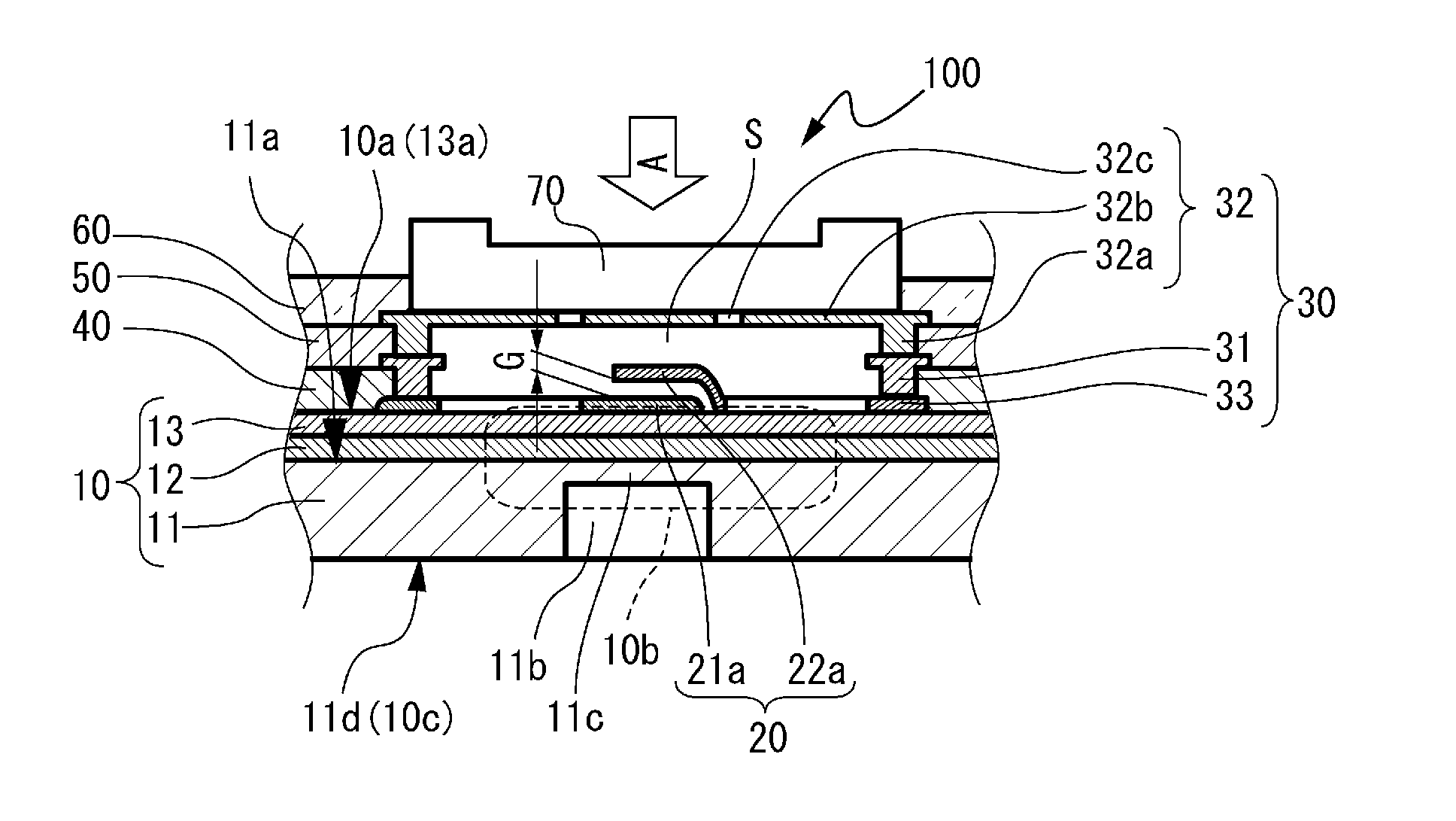
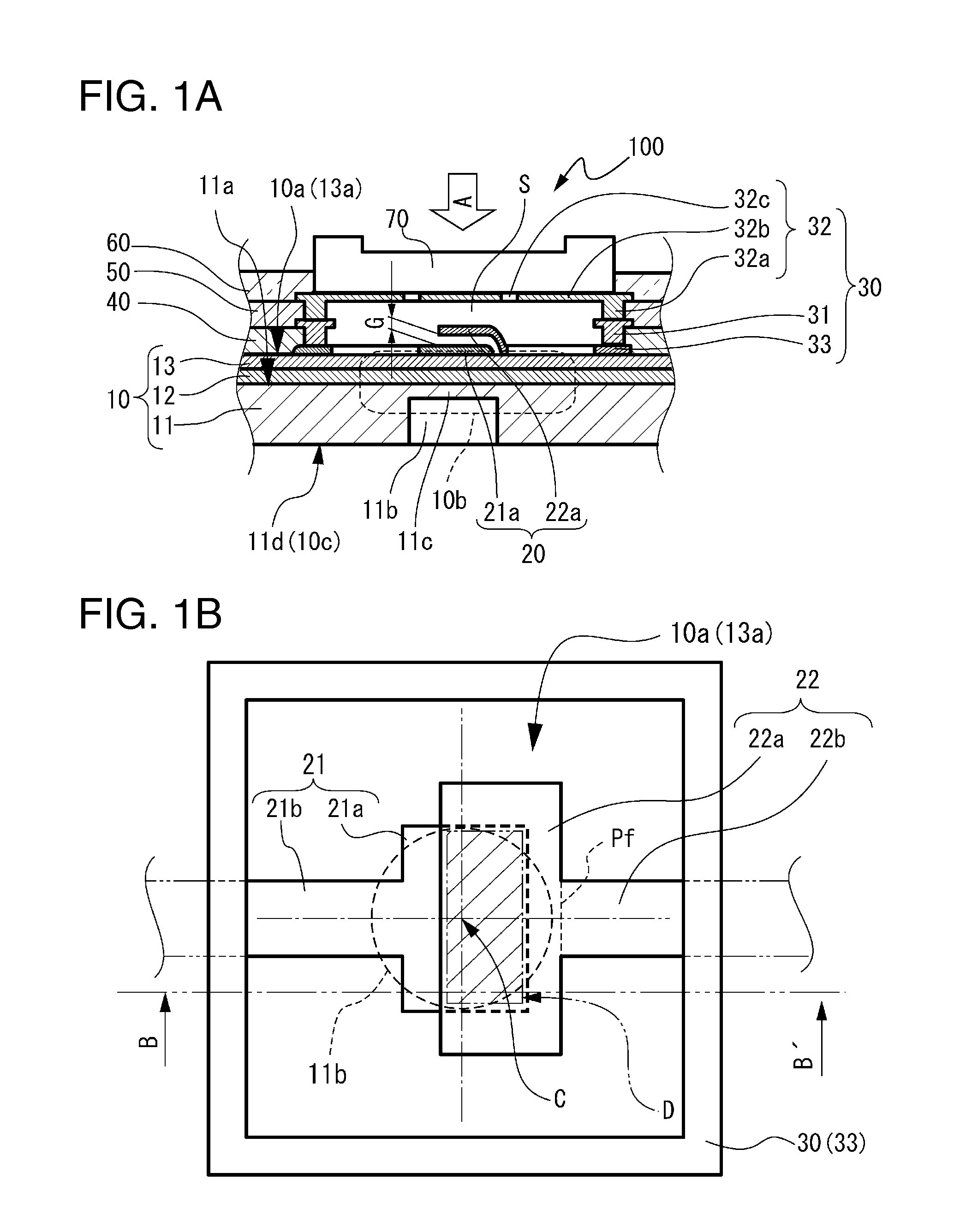
[0045]FIGS. 1A and 1B show a MEMS element according to a first embodiment, FIG. 1A is a schematic cross-sectional view, and FIG. 1B is a plan view in which a coating layer described below is transmitted when viewed from an A direction of an electrode portion shown in FIG. 1A. In addition, FIG. 1A is a cross-sectional view corresponding to a B-B′ portion shown in FIG. 1B. As shown in FIG. 1A, a MEMS element 100 according to the embodiment includes a substrate 10 configured of a wafer substrate 11, a first oxide film 12 which is formed on a principal surface 11a of the wafer substrate 11, and a nitride film 13 which is formed on the first oxide film 12. The wafer substrate 11 is a silicon substrate and is also used as the wafer substrate 11 which forms a semiconductor device described below, that is, a so-called IC.
[0046]A MEMS vibrator 20, which is a resonator, is formed on the principal surface 10a which is a first surface of the substrate 10, that is, a surface 13a of the nitride f...
second embodiment
[0065]As a second embodiment, an altimeter will be described with reference to the drawings. The altimeter according to the second embodiment is one form of an electronic apparatus including a pressure sensor which is an electronic device having the MEMS elements 100 and 200 according to the first embodiment.
[0066]As shown in FIG. 6A, an altimeter 1000 according to the second embodiment includes the MEMS element 200 according to the first embodiment, an element fixation frame 1200 which is a holding unit mounted on a housing 1100 to hold the MEMS element 200, and a calculation unit 1300 which calculates altitude data from the data signal obtained from the MEMS element 200, in the housing 1100. In the housing 1100, an opening 1100a is provided, through which the flexible portion 10b (refer to FIGS. 1A and 1B) of the MEMS element 100, which is included in the MEMS element 200, can be ventilated by the atmosphere.
[0067]An E portion shown in FIG. 6A, that is, the detail in the cross-sec...
third embodiment
[0072]A navigation system which is an electronic apparatus having the MEMS elements 100 and 200 according to the first embodiment or the altimeter 1000 according to the second embodiment, and a vehicle which is an aspect of a moving object on which the navigation system is mounted will be described.
[0073]FIG. 8 is an outline view of a vehicle 4000 which is the moving object including a navigation system 3000 as the electronic apparatus. The navigation system 3000 includes map information (not shown), a position information acquisition unit from a Global Positioning System (GPS), a self-contained navigation unit configured of a gyro sensor, an acceleration sensor, and vehicle speed data, and the altimeter 1000 according to the second embodiment, and displays the information in a predetermined position or road information on a display unit 3100 disposed at a position which can be viewed by a driver.
[0074]Since the altimeter 1000 is included in the navigation system 3000 in the vehicle...
PUM
 Abstract
Description
Claims
Application Information
 - R&D
- Intellectual Property
- Life Sciences
- Materials
- Tech Scout
- Unparalleled Data Quality
- Higher Quality Content
- 60% Fewer Hallucinations
Browse by: Latest US Patents, China's latest patents, Technical Efficacy Thesaurus, Application Domain, Technology Topic, Popular Technical Reports.
© 2025 PatSnap. All rights reserved.Legal|Privacy policy|Modern Slavery Act Transparency Statement|Sitemap|About US| Contact US: help@patsnap.com


