
Electrostatic Capacitance Type Touch Panel and Anti-Glare Film

a capacitance type, touch panel technology, applied in the direction of pulse technique, electric apparatus casing/cabinet/drawer, instruments, etc., can solve the problems of fingerprints to be adhered by touching, the tendency of fingerprints to become noticeable, and the difficulty in satisfying both anti-glare properties

Inactive Publication Date: 2014-05-29
KIMOTO CO LTD
View PDF4 Cites 13 Cited by
  • Summary
  • Abstract
  • Description
  • Claims
  • Application Information

AI Technical Summary

Benefits of technology

The present invention provides an electrostatic capacitance type touch panel with anti-glare properties and low visibility of fingerprints. This can be achieved by providing a surface with specific conditions that suppress adhesion of fingerprints and make fingerprints less noticeable. The invention also provides an anti-glare film with low visibility of fingerprints that can be used on the operating surface of a touch panel or a display screen for a display device. Overall, the invention provides a solution for improved accessibility and aesthetics for electronic devices.

Problems solved by technology

However, when touching an electronic device provided with an anti-glare film with a higher roughness degree on the textured surface as such, there was a tendency that adhered fingerprints become noticeable.
Although to roughen a surface of an anti-glare film is necessary to develop anti-glare properties as explained above, fingerprints to be adhered by touching tend to become noticeable.
Therefore, it has been difficult to satisfy both of the anti-glare properties and an effect of obscuring fingerprints (low visibility of fingerprints) only by simply roughening the surface of the anti-glare film.
Due to this, also as to touch panels having a surface provided with an anti-glare film as above, it has been difficult to satisfy anti-glare properties and the low visibility of fingerprints at the same time.

Method used

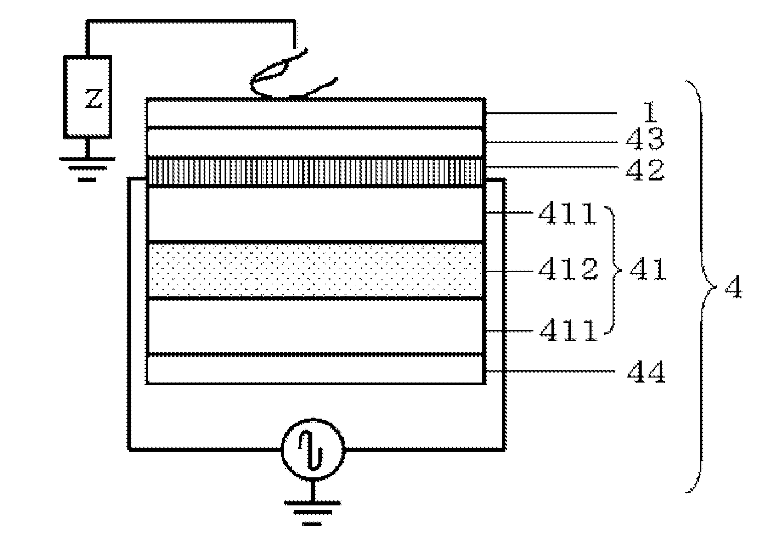
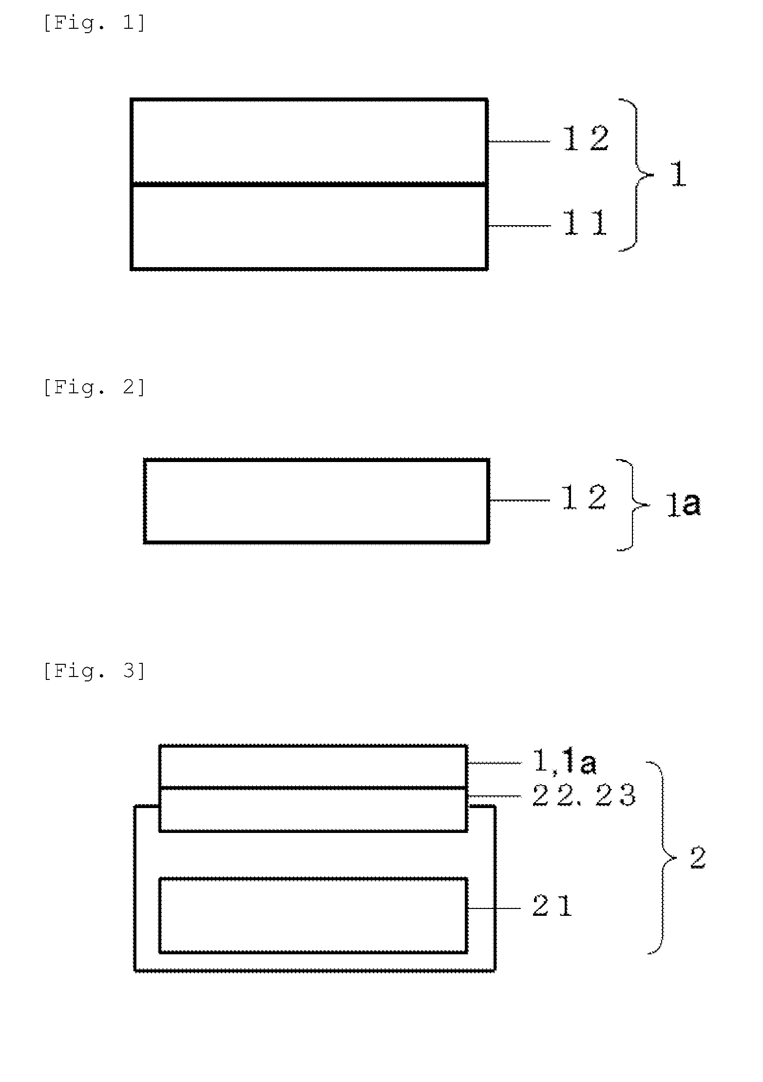
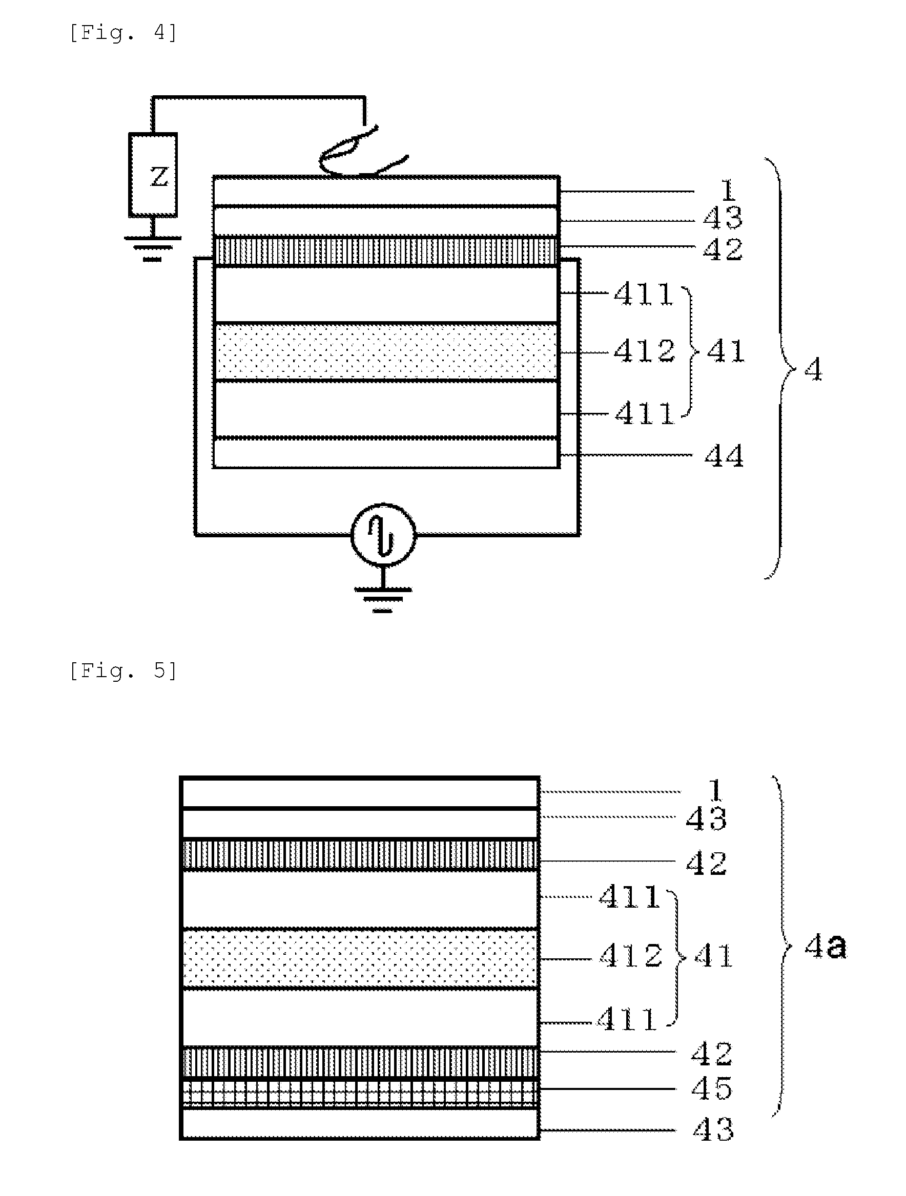

Image

  • Electrostatic Capacitance Type Touch Panel and Anti-Glare Film
  • Electrostatic Capacitance Type Touch Panel and Anti-Glare Film
  • Electrostatic Capacitance Type Touch Panel and Anti-Glare Film

Examples


example 1

[0098]On one surface of a transparent polyester film having a thickness of 125 μm (COSMOSHINE A4350), an anti-glare layer application liquid ‘a’ of the prescription below was applied, dried and irradiated with an ultraviolet ray so as to form an anti-glare layer having a thickness of 6 μm, so that an anti-glare film of the example 1 was obtained.

[0099]ionizing radiation curable type resin composition 200 parts[0100](DeSolite 7501: JSR Corporation, Solid content 50%)

photopolymerization initiator 1 part[0101](IRGACURE 651: Ciba Japan K. K.)

silica 8.5 parts[0102](OK-500: DEGUSSA CORP)[0103](average particle diameter: 3.0 μm, specific weight: 1.9)

diluting solution 200 parts

example 2

[0104]Other than forming an anti-glare layer having a thickness of 5 μm by changing the application condition, an anti-glare film of an example 2 was obtained in the same way as in the example 1.


PUM

PropertyMeasurementUnit
contact angleaaaaaaaaaa
hazeaaaaaaaaaa
hazeaaaaaaaaaa

Abstract

Provided is an electrostatic capacitance type touch panel (4) having an operating surface that is provided with anti-glare properties and low visibility of fingerprints. A textured surface satisfying all of the following conditions ‘a’ to ‘d’ is provided on the operating surface side of the electrostatic capacitance type touch panel (4). Condition ‘a’: Ra (arithmetic mean roughness) of 0.1-0.5 μm. Condition ‘b’: RΔq (root-mean-square gradient) of 2° or greater. Condition ‘c’: Rsm (mean spacing between profile peaks) of 0.1 mm or less. Condition ‘d’: Rp (maximum peak height) of 1.0 μm or less. All of these values are measured in accordance with JIS B0601:2001.

Description

TECHNICAL FIELD[0001]The present invention relates to an electrostatic capacitance type touch panel having anti-glare properties. The present invention also relates to an anti-glare film used for a film adhered to a surface of a variety of devices and a film for other touch panels, etc.BACKGROUND ART[0002]A transparent film for surface protection is often adhered to a surface of a variety of devices (liquid crystal display devices, showcases and cover glasses of clocks and instruments, etc.).[0003]In recent years, as typified by ATMs of banks and ticket vending machines, electronic devices provided with a touch panel type liquid crystal monitor have been increasing. As a surface protection transparent film of such liquid crystal monitors and a transparent film used for touch panels, anti-glare films are used, on which a surface texture treatment is performed to prevent difficulty in seeing caused by glare due to reflections of external lights.[0004]To enhance the anti-glare effect o...

Claims


Application Information

Patent Timeline
Patent Type & Authority Applications(United States)
IPC IPC(8): G02B1/11H05K7/00H03K17/96
CPCG02B1/118G02B5/0226G02B5/0263G02B5/0278G06F3/0445G02F1/1335H03K17/962H05K7/00G02B1/11
Inventor NOZAWA, KAZUHIRO
Owner KIMOTO CO LTD
Learn More