Cross point variable resistance nonvolatile memory device

a non-volatile, memory device technology, applied in the direction of information storage, static storage, digital storage, etc., to achieve the effect of fast operation, stable writing operation, and easy manufactur

Active Publication Date: 2014-04-10
PANASONIC SEMICON SOLUTIONS CO LTD
View PDF3 Cites 43 Cited by
  • Summary
  • Abstract
  • Description
  • Claims
  • Application Information

AI Technical Summary

Benefits of technology

The present invention is about a cross point variable resistance nonvolatile memory device with a unique feature of bidirectional current limiting that makes it easy to manufacture and operate. The device can be written to the low or high resistance state with a limited amount of current regardless of which layer it is accessed from. This ensures stable writing operation in all layers and allows for fast operations and mass memory suitable for various information devices. Overall, this invention has practical value and is useful for memory devices in various information devices.

Problems solved by technology

However, PTL 3 does not disclose such a writing method as described in PTL 2 in which, when changing a programmable resistance element from the high resistance state to the low resistance state, a predetermined constant current that enables a resistance change is caused to flow through the programmable resistance element to thereby change the programmable resistance element to a resistance state of a low resistance value corresponding to the value of the current.

Method used


Image

  • Cross point variable resistance nonvolatile memory device
  • Cross point variable resistance nonvolatile memory device
  • Cross point variable resistance nonvolatile memory device

Examples


reference example 1

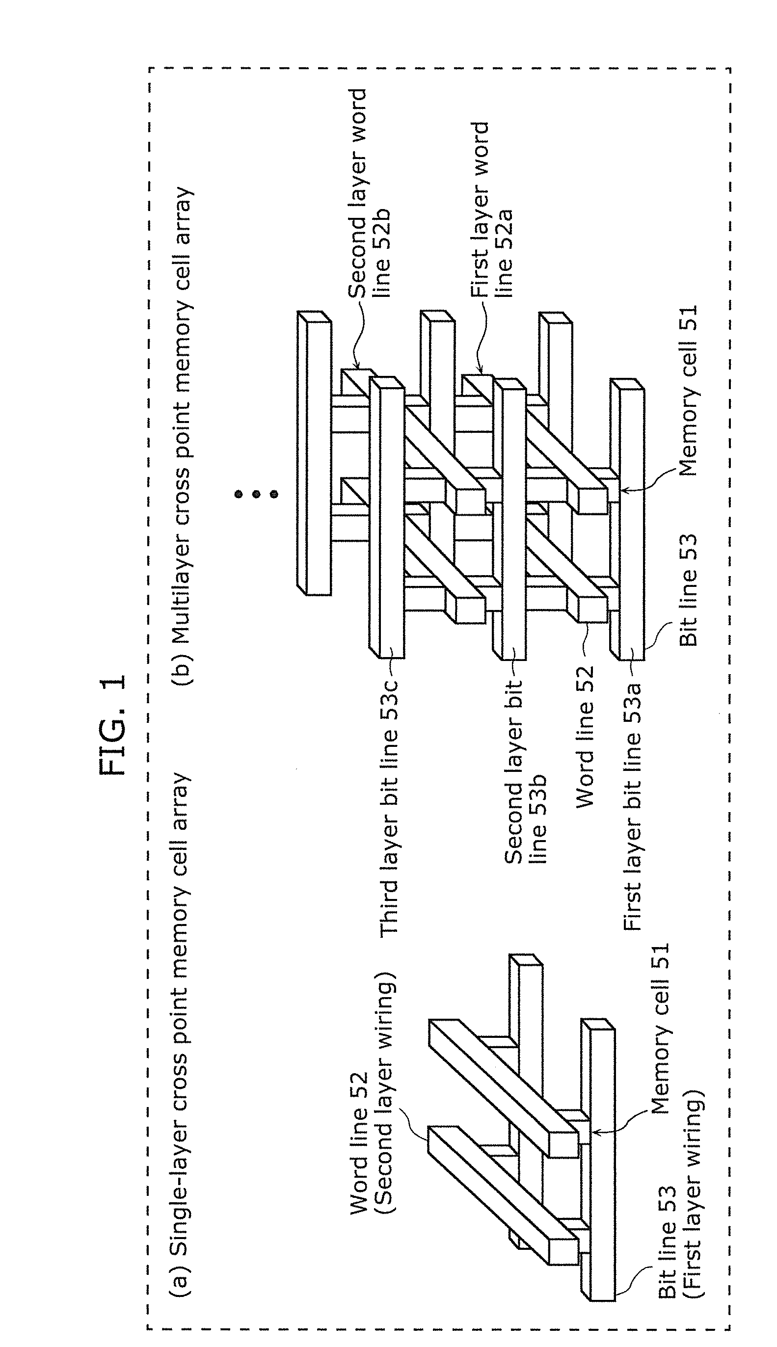
Description of Circuit Structure

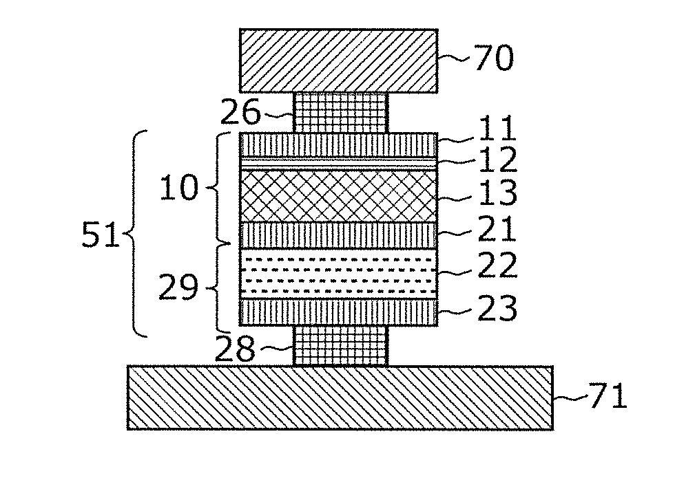
[0151]FIG. 10 is a diagram showing a cross section structure of a memory cell 51 included in a cross point variable resistance nonvolatile memory device having a multilayer memory cell array in Reference Example 1.

[0152]The memory cell 51 has a structure in which a first electrode 23 comprising tantalum nitride (TaN), a current steering layer 22 comprising nitrogen-deficient silicon nitride, a second electrode 21 comprising TaN, a first variable resistance layer 13 comprising oxygen-deficient tantalum oxide (TaOx), a second variable resistance layer 12 formed by oxidation of the first variable resistance layer 13 in an oxygen plasma atmosphere and comprising TaOy (xx, and a third electrode 11 comprising platinum (Pt) are stacked in this order. A lower wire 71 comprising aluminum (Al) is disposed below the memory cell 51, and connected to the first electrode 23 of the memory cell 51 by a first via 28. An upper wire 70 comprising aluminum (Al) is dispos...

reference example 2

[0376]In Reference Example 1, in the operation of writing to the multilayer cross point nonvolatile memory device, only one transistor out of the N-type current limiting element 90 and the P-type current limiting element 91 that has a greater substrate bias effect in a direction in which a current for low resistance writing flows through the memory cell is activated depending on the writing target memory array layer to which the memory cell belongs, to thereby perform the low resistance writing operation. In such low resistance writing, the current flow is limited in the source follower operation mode (i.e. the source follower mode).

[0377]Reference Example 2 is based on the same structure in which the N-type current limiting element 90 and the P-type current limiting element 91 are included, but differs in control method. Depending on the writing target memory array layer, a desired gate voltage is applied to the gate terminal of each of the N-type current limiting element 90 and th...

modification 1

[Modification 1]

[0557]FIG. 27 is a diagram showing a structure in which the threshold voltages Vt of the MOS transistors in the N-type current limiting element 90 and the P-type current limiting element 91 are adjusted to 0 V in the structure shown in FIG. 11 (such N-type current limiting element and P-type current limiting element are respectively referred to as an N-type current limiting element 90a and a P-type current limiting element 91a). In this modification, the threshold voltage of the N-type current limiting element 90 is referred to as a third threshold voltage, the threshold voltage of the P-type current limiting element 91 as a fourth threshold voltage, the threshold voltage of the other NMOS transistors as a first threshold voltage, and the threshold voltage of the other PMOS transistors as a second threshold voltage. Changing the threshold voltage Vt only for a predetermined transistor can be easily realized by a generally known method such as providing a mask only in...


PUM


Abstract

Each memory cell is formed at a different one of cross points of bit lines extending in an X direction and formed in a plurality of layers and word lines extending in a Y direction. In a multilayer cross point structure in which a plurality of vertical array planes sharing the word lines are aligned in the Y direction each for a group of bit lines aligned in a Z direction, even and odd layer bit line selection switch elements switch connection and disconnection between a global bit line and the commonly-connected even layer bit line and the commonly-connected odd layer bit line, respectively. Each of the even and odd layer bit line selection switch elements has both a bit line selection function and a current limiting function in low resistance writing.

Description

TECHNICAL FIELD[0001]The present invention relates to a nonvolatile memory device having cross point memory cells that include variable resistance elements.BACKGROUND ART[0002]In recent years, research and development are conducted on a nonvolatile memory device having memory cells that include variable resistance elements. A variable resistance element is an element that has a property of changing in resistance value (changing between a high resistance state and a low resistance state) according to an electrical signal and enables information to be written by this change in resistance value.[0003]One structure of memory cells using variable resistance elements is a cross point structure. In the cross point structure, each memory cell is formed at a different one of cross points of orthogonally arranged bit lines and word lines so as to be positioned between a bit line and a word line. Various types of such cross point variable resistance nonvolatile memory devices are developed in ...

Claims


Application Information

Patent Timeline
IPC IPC(8): G11C13/00
CPCG11C13/0002G11C13/0069G11C13/004G11C13/0007G11C13/0023G11C2213/71G11C13/0026G11C2213/77H10B63/22H10B63/84H10N70/24H10N70/826H10N70/8833
Inventor AZUMA, RYOTAROSHIMAKAWA, KAZUHIKO
Owner PANASONIC SEMICON SOLUTIONS CO LTD
Why Eureka
Try Eureka