Solid-state imaging apparatus with plural readout modes, and electronic equipment
a solid-state imaging and readout mode technology, applied in the direction of television systems, radio frequency controlled devices, instruments, etc., can solve the problems of degrading resolution and long sideways images, and achieve the reduction of the number of signals in the horizontal direction, the reduction of the angle of view, and the increase of the frame rate.
- Summary
- Abstract
- Description
- Claims
- Application Information
AI Technical Summary
Benefits of technology
Problems solved by technology
Method used
Image
Examples
first embodiment
2. First Embodiment
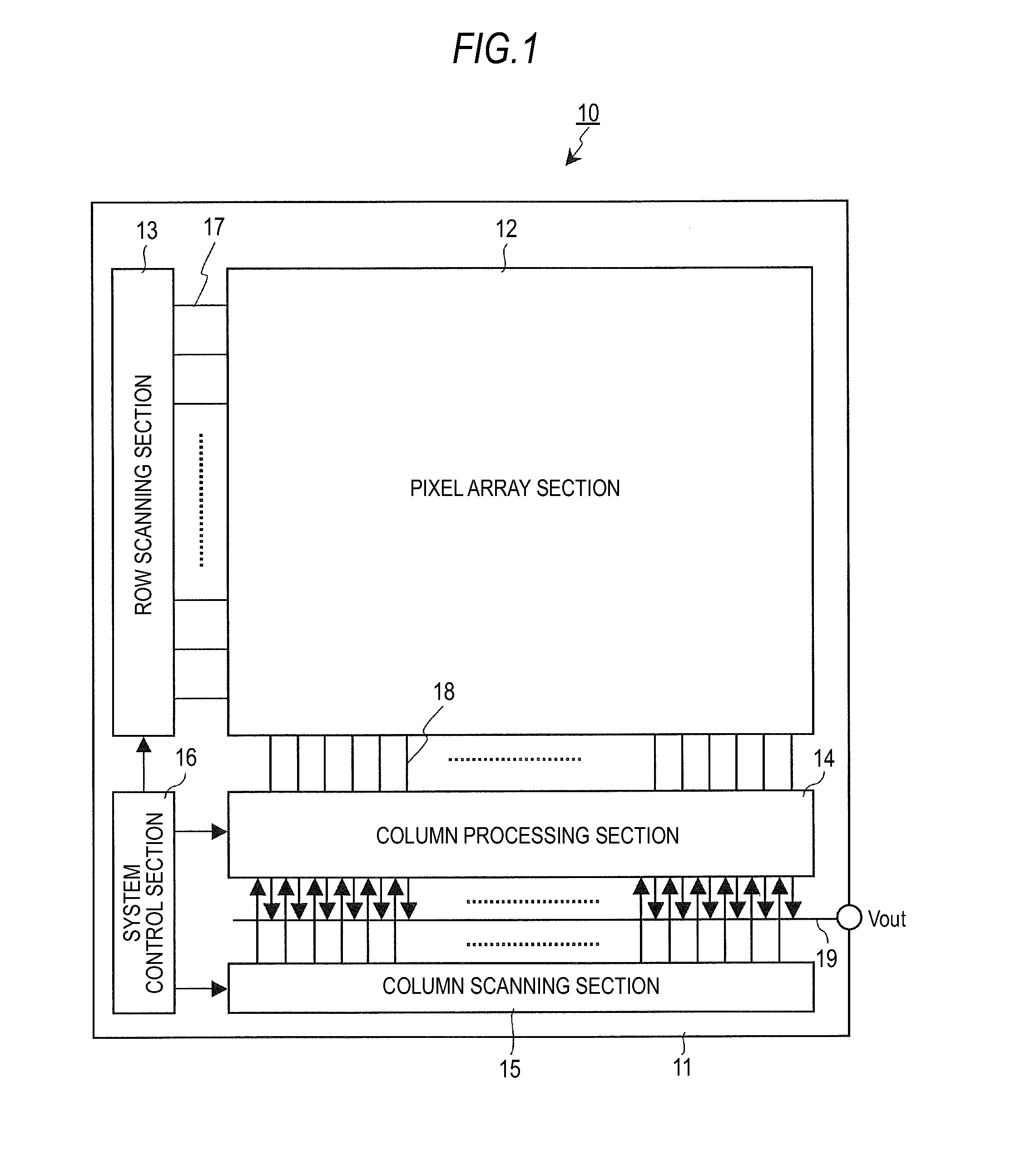
[0064]FIG. 3 is a system structural view showing the outline of a system structure of a CMOS image sensor 10A of a first embodiment of the invention. In the drawing, the same portion as that of FIG. 1 is denoted by the same reference numeral.
[0065]The CMOS image sensor 10A of this embodiment is constructed such that plural, for example, two systematic pixel drive lines 17 are arranged for each pixel row. Unit pixels 20 are connected to the two systematic pixel drive lines 17A and 17B in units of two adjacent columns. Specifically, the connection relation is such that from the left in the drawing, the respective pixels 20 of the first pixel column and the second pixel column are connected to the pixel drive line 17A, the respective pixels 20 of the third pixel column and the fourth pixel column are connected to the pixel drive line 17B, the respective pixels 20 of the fifth pixel column and the sixth pixel column are connected to the pixel drive line 17A, and so on...
second embodiment
3. Second Embodiment
[0105]FIG. 10 is a system structural view showing the outline of a system structure of a CMOS image sensor 10B of a second embodiment. In the drawing, the same portion as that of FIG. 3 is denoted by the same reference numeral.
[0106]The CMOS image sensor 10B of this embodiment has a structure in which plural, for example, two systematic (two lines) vertical signal lines 18 are arranged for each pixel column. Unit pixels 20 are alternately connected to the two systematic vertical signal lines 18A and 18B for the respective pixel rows. Specifically, the connection relation is such that each of the pixels 20 of the first pixel row from above in the drawing is connected to the vertical signal line 18A, and each of the pixels 20 of the second pixel row is connected to the vertical signal line 18B, each of the pixels 20 of the third pixel row is connected to the vertical signal line 18A, and so on.
[0107]One systematic pixel drive line 17 is arranged for each pixel row....
third embodiment
4. Third Embodiment
[0136]FIG. 13 is a system structural view showing the outline of a system structure of a CMOS image sensor 10C of a third embodiment. In the drawing, the same portion as that of FIG. 10 is denoted by the same reference numeral.
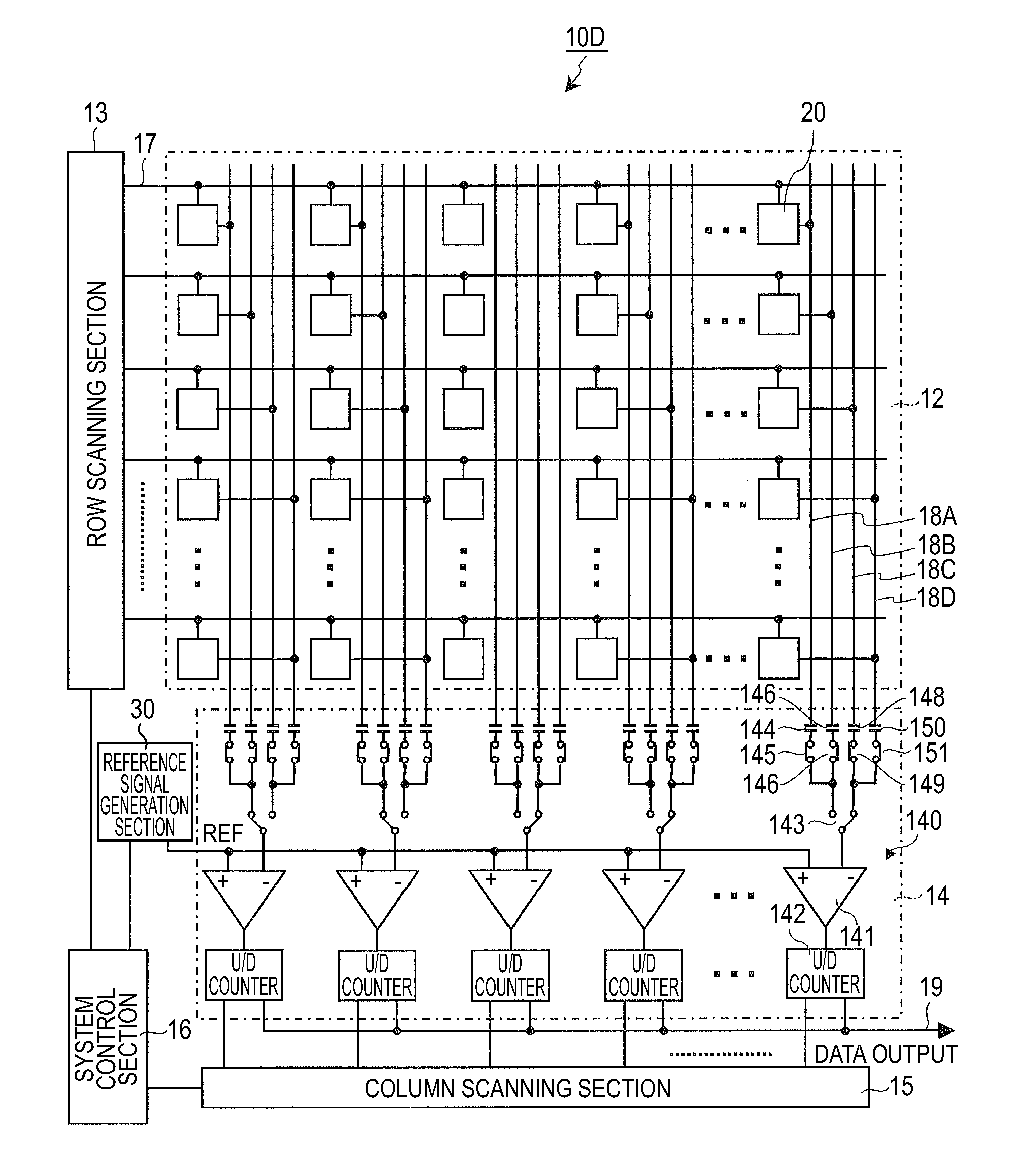
[0137]In the CMOS image sensor 10B of the second embodiment, for example, the two systematic vertical signal lines 18A and 18B are arranged for each pixel column. Then, the vertical signal lines 18A and 18B are alternately selected in units of two adjacent columns by the selection switch 143, and the signals are read out simultaneously from the pixels 20 of two pixel rows for different pixel columns, so that the horizontal thinning-out readout is performed while the vertical thinning-out readout is performed.
[0138]The CMOS image sensor 10C of this embodiment is the same as the CMOS image sensor 10B of the second embodiment in that plural, for example, two systematic vertical signal lines 18A 18B are provided for each pixel column, and signal...
PUM
 Abstract
Description
Claims
Application Information
 - R&D
- Intellectual Property
- Life Sciences
- Materials
- Tech Scout
- Unparalleled Data Quality
- Higher Quality Content
- 60% Fewer Hallucinations
Browse by: Latest US Patents, China's latest patents, Technical Efficacy Thesaurus, Application Domain, Technology Topic, Popular Technical Reports.
© 2025 PatSnap. All rights reserved.Legal|Privacy policy|Modern Slavery Act Transparency Statement|Sitemap|About US| Contact US: help@patsnap.com


