Recovery of silicon value from kerf silicon waste

a technology of kerf silicon and waste, which is applied in the field of recovery of silicon value, can solve the problems of kerf silicon waste, high energy consumption of process, and significant silicon waste of wire saw process, and achieve the effect of high purity of kerf silicon

Inactive Publication Date: 2013-12-05
SEMLUX TECH
View PDF4 Cites 15 Cited by
  • Summary
  • Abstract
  • Description
  • Claims
  • Application Information

AI Technical Summary

Benefits of technology

[0013]It is an object of the invention to provide a viable and practical industrial process and technology to recover kerf silicon powder waste into a form that has an appropriate level of purity for use as silicon feed stock for different applications. It is a further object to provide a process and technology that will maintain the intrinsic high purity of the kerf silicon.

Problems solved by technology

The processes, collectively called the Siemens Process, are very energy intensive.
This wire saw process produces significant silicon waste, known as kerf silicon waste, due to the cutting of the silicon ingot or block.
Slicing silicon ingot or block to make wafers is one of the most expensive and wasteful process steps in the silicon value chain, especially in the PV cell manufacturing industry.
This adds significantly to the silicon shortage of the PV industry.
All these contribute to higher PV cell manufacturing costs and wasted energy.
The semiconductor and solar industries cannot afford to dispose off such valuable materials without environmental concerns.
There is no practical process in the industry to recover silicon from the kerf waste and produce high purity silicon at competitive costs.
The few development efforts such as the project RE-Si-CLE [ENK5-CT2001-00567 (2002-04)], iodide transport [PCT / US2009 / 040261], melt refining [Photovoltaic Specialists Conference, June 2010], etc. are academic in that industrialization is challenging or impractical.
Kerf material pretreatment procedures [USPTO Applications 20100163462 and 20100284885] attempt near complete separation of kerf silicon from SiC and metal impurities; however, the Si purity is insufficient for PV applications.

Method used


Image

  • Recovery of silicon value from kerf silicon waste
  • Recovery of silicon value from kerf silicon waste
  • Recovery of silicon value from kerf silicon waste

Examples


example 1

Pretreatment of Kerf Silicon

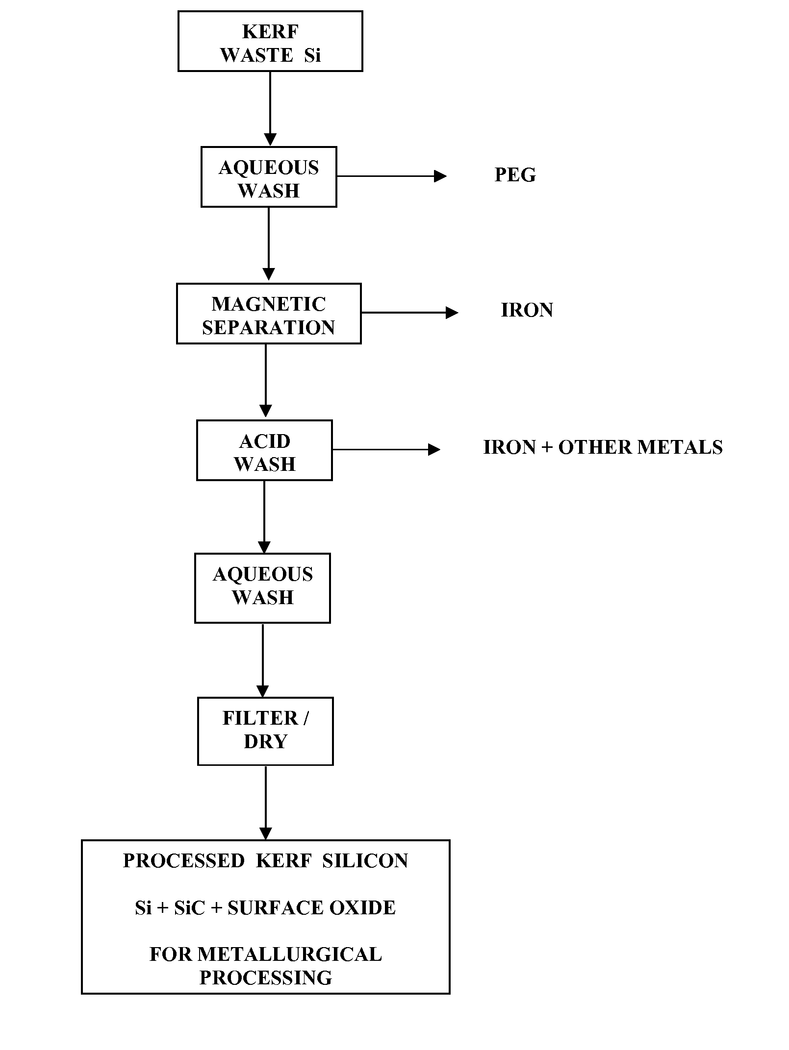
[0088]Kerf silicon typically contains 50-60% Si, 25-30% SiC, 5-10% oxidized Si, 4-5% Fe, approximately 0.1% Cu and Zn and traces of other metallic impurities added from the slurry recovery and kerf silicon separation processes. Typical levels of impurities in kerf Si are: Fe˜4-5%, Al 250-300 ppm, Ca 500-700 ppm, Ti 5-100 ppm,

[0089]Mn 100-200 ppm, Na 0.1%, Cu ˜0.2%, Zn ˜0.1%, traces of alkali metals.

[0090]B<2 ppm, P ˜0 ppm. Almost all of these impurities are extrinsic to the silicon, since the latter was derived from crystal grown ingots. As such, the levels of these impurities can be controlled and reduced by proper care in the slurry recovery and kerf separation processes. They can also be removed by appropriate pretreatment of the kerf silicon waste.

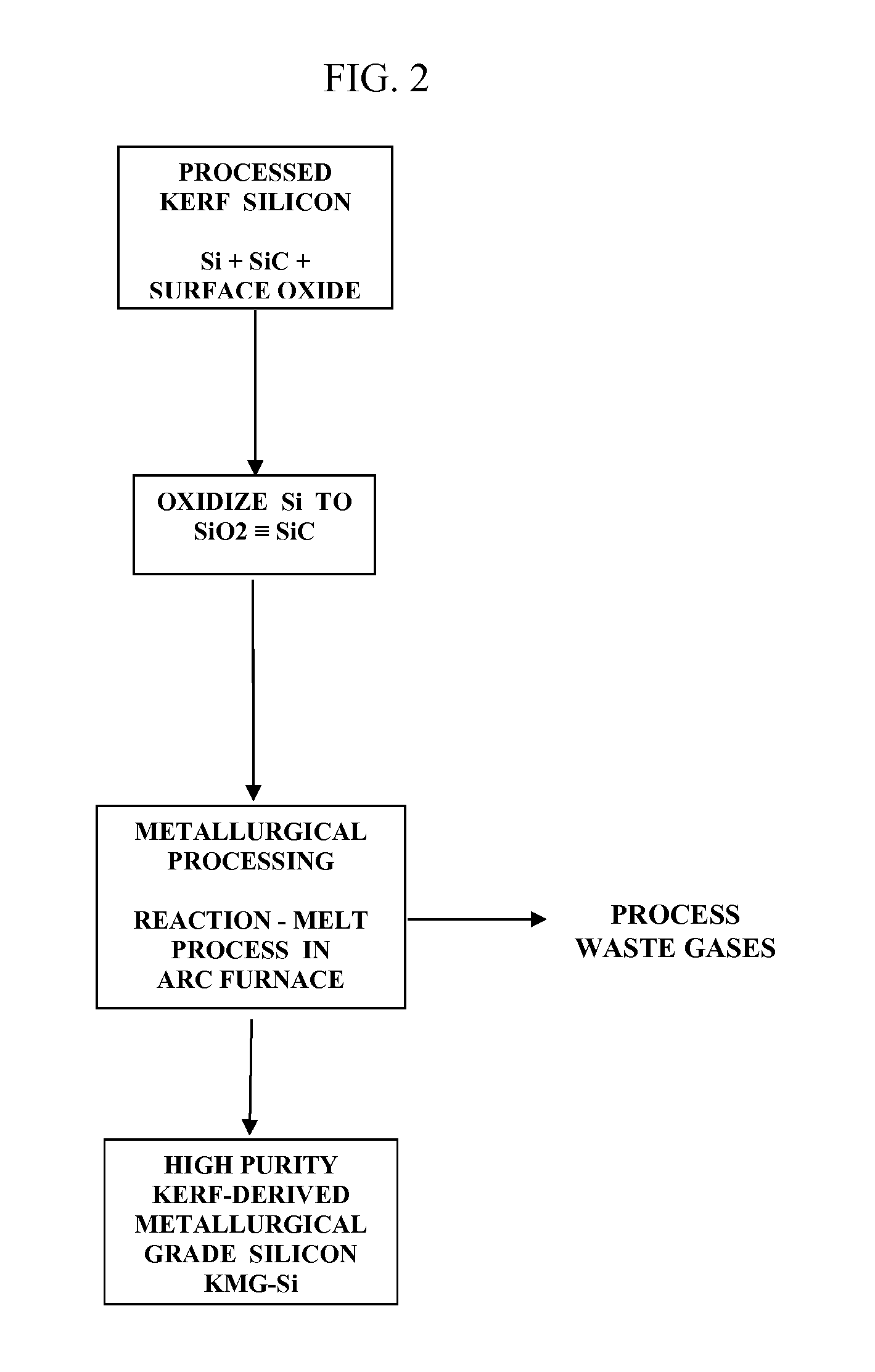
[0091]Since these impurities are present as metals or their oxides, acid extraction is the most appropriate pretreatment process. In an example the kerf silicon was treated by leaching the impurities with a ...


PUM

PropertyMeasurementUnit
purityaaaaaaaaaa
abrasiveaaaaaaaaaa
metallic impuritiesaaaaaaaaaa

Abstract

The present invention is for the recovery of maximum silicon value of kerf silicon waste, produced during the manufacture of silicon wafers by wire saw, diamond saw and chemical mechanical polishing, as high purity metallurgical silicon. This recovery is achieved by a process scheme that effects an initial removal of minor extrinsic metallic impurities but not the major silicon compound impurities, and followed, preferentially, by a direct metallurgical process to form elemental silicon. The recovered silicon is for use as feedstock for polysilicon manufacturing, as high purity polysilicon for PV application, and in metallurgical alloy manufacture.

Description

RELATED APPLICATIONS[0001]This application is a continuation of PCT Patent Application No. U.S.12 / 24511, filed Feb. 9, 2012, and entitled “RECOVERY OF SILICON VALUE FROM KERF SILICON WASTE”, which application claims the benefit of U.S. Provisional Application No. 61 / 462,905, filed Feb. 9, 2011 and entitled “RECOVERY OF SILICON VALUE FROM KERF SILICON WASTE”, the entire content of which are incorporated herein by reference.INCORPORATION BY REFERENCE[0002]All patents, patent applications and publications cited herein are hereby incorporated by reference in their entirety in order to more fully describe the state of the art as known to those skilled therein as of the date of the invention described herein.BACKGROUND OF THE INVENTION[0003]The current mainstream method for producing high purity polysilicon for the electronic and photovoltaic (PV) industries is a combination of metallurgical and chemical. Starting from pure quartz (SiO2), metallurgical grade silicon (MG-Si) is made by car...

Claims


Application Information

Patent Timeline
Patent Type & Authority Applications(United States)
IPC IPC(8): C01B33/023B28D5/00
CPCC01B33/023B28D5/0005C01B33/037C01B33/10736C01B33/10763C01B33/039B28D5/045
Inventor HARIHARAN, ALLEPPEY V.RAVI, JAGANNATHAN
Owner SEMLUX TECH
Why Eureka
Try Eureka