Multi-chip package and operating method thereof

a technology of multi-chips and operating methods, applied in the field of semiconductor design technology, can solve problems such as voltage drop, circuit malfunction, and error related to peak current raised

Active Publication Date: 2013-11-21
SK HYNIX INC
View PDF5 Cites 1 Cited by
  • Summary
  • Abstract
  • Description
  • Claims
  • Application Information

AI Technical Summary

Benefits of technology

The present invention is about a multi-chip package system that can control the operations of multiple semiconductor chips. The system includes a controller that generates an enable control signal to select one of the semiconductor chips to perform a specific operation based on their current consumption. The enable control signal is circulated through all the semiconductor chips to control their operations. The system allows for efficient performance and operation management of the multiple semiconductor chips.

Problems solved by technology

As semiconductor devices have been miniaturized, an error related to a peak current has been raised.
At this time, when a peak current occurs, a voltage drop occurs to cause a malfunction of the circuit.
Particularly in a multichip package, when operation periods of a plurality of semiconductor chips overlap each other, a peak current may occur to cause a voltage drop.
In this case, the voltage drop may cause a malfunction of the multi-chip package as well as malfunctions of some semiconductor chips.

Method used


Image

  • Multi-chip package and operating method thereof
  • Multi-chip package and operating method thereof
  • Multi-chip package and operating method thereof

Examples


Embodiment Construction

[0017]Exemplary embodiments of the present invention will be described below in more detail with reference to the accompanying drawings. The present invention may, however, be embodied in different forms and should not be construed as limited to the embodiments set forth herein. Rather, these embodiments are provided so that this disclosure will be thorough and complete, and will fully convey the scope of the present invention to those skilled in the art. Throughout the disclosure, like reference numerals refer to like parts throughout the various figures and embodiments of the present invention.

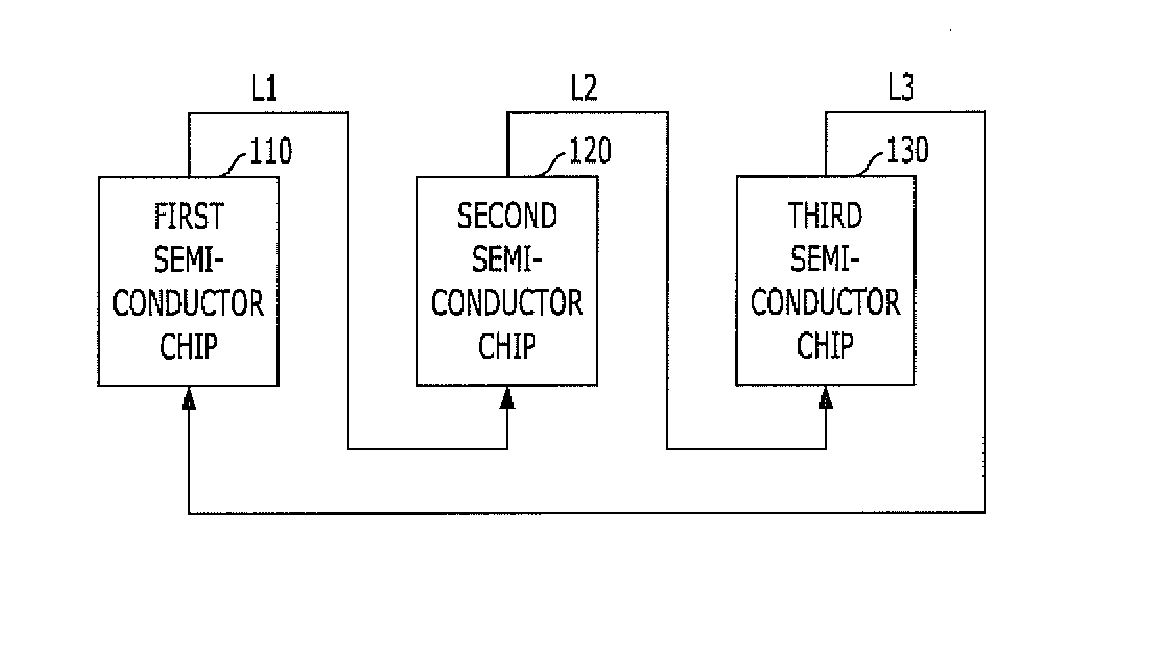
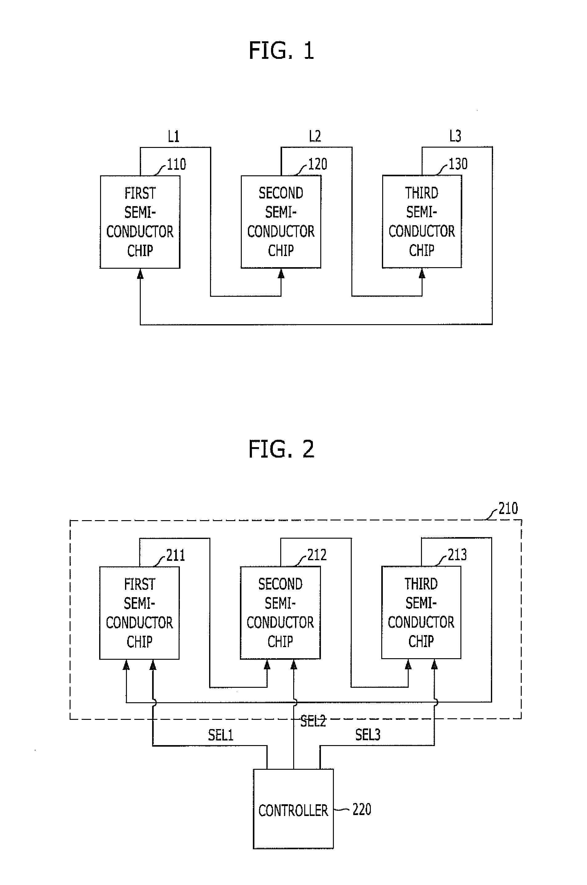
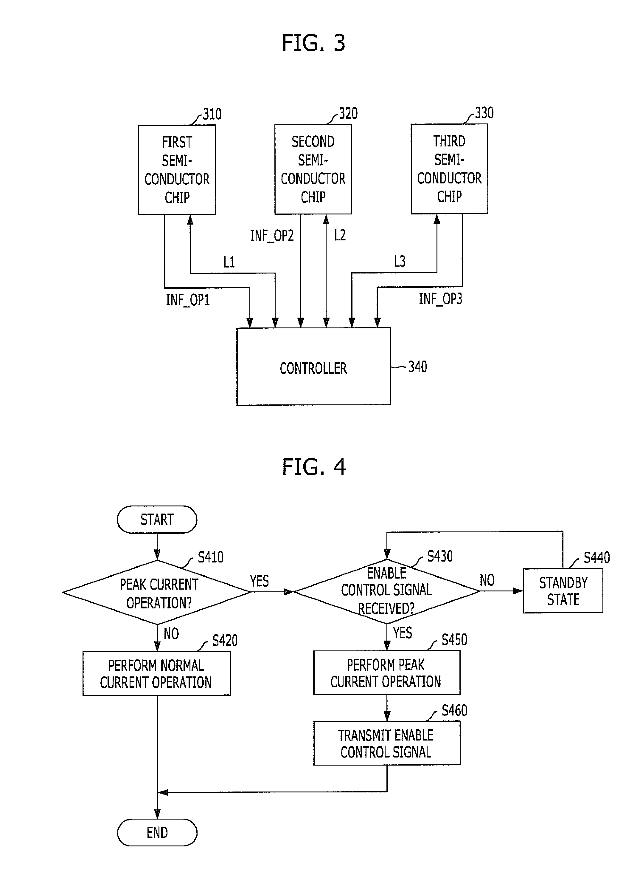
[0018]FIG. 1 is a block diagram explaining the configuration of a multi-chip package in accordance with an exemplary embodiment of the present invention. For the illustrative purposes, FIG. 1 illustrates the multi-chip package including three semiconductor chips.

[0019]Referring to FIG. 1, the multi-chip package includes a first semiconductor chip 110, a second semiconductor chip 120, and a t...


PUM


Abstract

A multi-chip package includes first and second semiconductor chips each configured to perform first and second operations having different current consumptions. The first and second semiconductor chips perform the first operation in response to an enable control signal transmitted from one of the first and second semiconductor chips to the other and transmitted from the other back to the one.

Description

CROSS-REFERENCE TO RELATED APPLICATIONS[0001]The present application claims priority of Korean Patent Application No. 10-2012-0053742, filed on May 21, 2012, which is incorporated herein by reference in its entirety.BACKGROUND[0002]1. Field[0003]Exemplary embodiments of the present invention relate to semiconductor design technology, and more particularly, to a multi-chip package including a plurality of semiconductor chips.[0004]2. Description of the Related Art[0005]In general, semiconductor devices including DDR SDRAM (Double Data Rate Synchronous DRAM) are developing to satisfy users' various needs. For such a development direction, package technology of semiconductor devices has been proposed. For example, a multi-chip package has been developed as the package technology. The multi-chip package refers to a structure for forming one single chip using a plurality of semiconductor chips. Depending on the configurations of the multi-chip package, a plurality of semiconductor chips ...

Claims


Application Information

Patent Timeline
Patent Type & Authority Applications(United States)
IPC IPC(8): H01L25/16H03H11/02H01L23/48
CPCG11C5/14G11C5/02G11C7/10G11C7/22
Inventor KANG, WON-KYUNGWON, SAM-KYU
Owner SK HYNIX INC
Why Eureka
Try Eureka