Variable resistance memory device and method for fabricating the same
a memory device and variable resistance technology, applied in semiconductor/solid-state device manufacturing, basic electric elements, electric devices, etc., can solve the problems of increasing fabrication costs and complicated fabrication processes, and achieve the effect of simplifying the manufacturing process, reducing the number of mask processes, and increasing the integration degree of memory cells
- Summary
- Abstract
- Description
- Claims
- Application Information
AI Technical Summary
Benefits of technology
Problems solved by technology
Method used
Image
Examples
first embodiment
[0049]By the fabrication method as described above, the variable resistance memory device in accordance with the present invention as shown in FIG. 1J may be fabricated.
[0050]Referring to FIG. 1J, the variable resistance memory device in accordance with the first embodiment may include the first vertical electrodes 125 which vertically project from the substrate 100 the plurality of first interlayer dielectric layer patterns 105A and the plurality of horizontal electrodes 130 which are alternately stacked along the first vertical electrodes 125, the first variable resistance layer 120 which is interposed between the first vertical electrodes 125 and the first horizontal electrodes 130, the second vertical electrodes 160 which are connected with the first vertical electrodes 125 and extend in the direction perpendicular to the substrate 100, the plurality of second interlayer dielectric layer patterns 145A and the plurality of second horizontal electrodes 165 which are alternately st...
second embodiment
[0071]In the second embodiment, since a variable resistance layer is formed after forming horizontal electrodes, it is possible to prevent the variable resistance layer from being damaged in the course of removing sacrificial layer patterns.
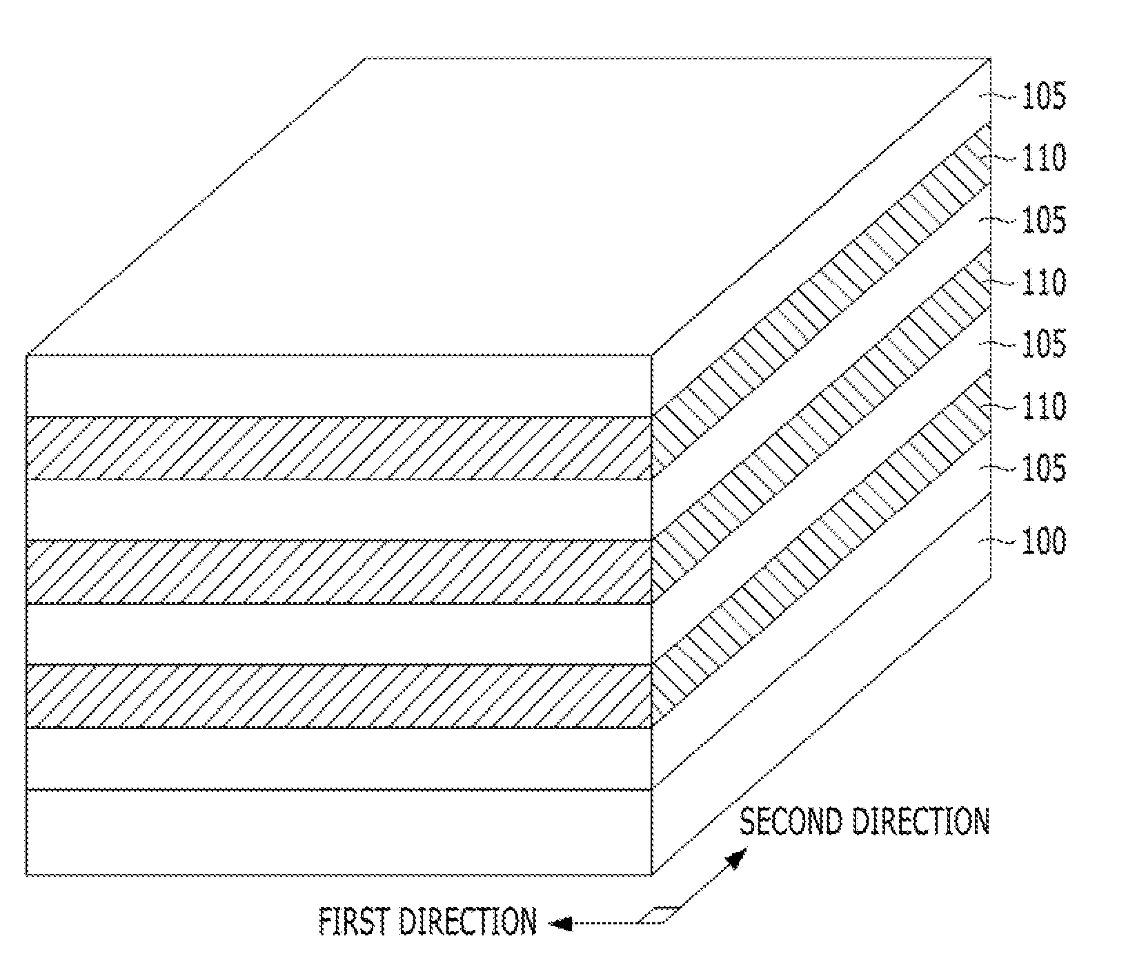
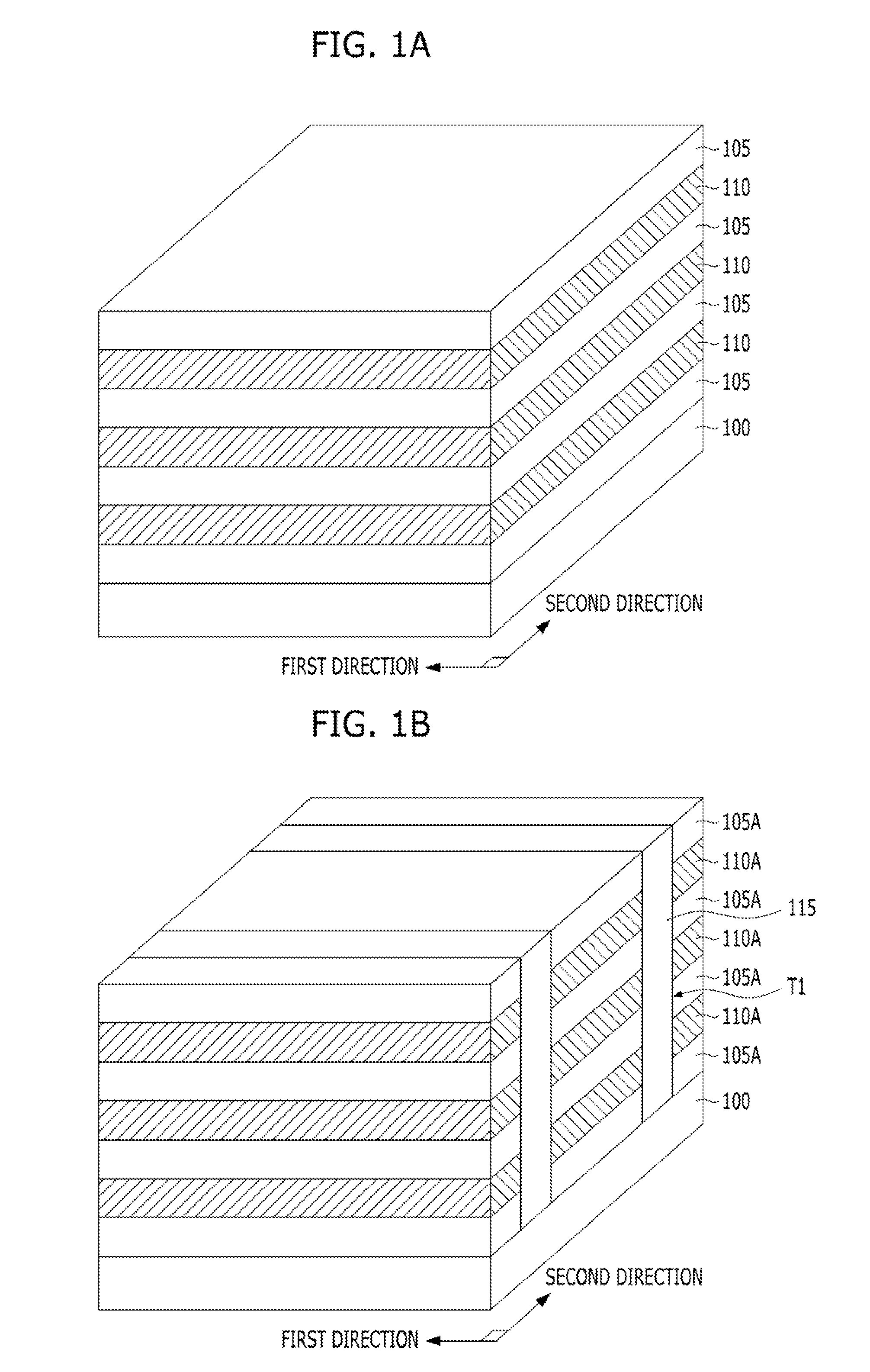
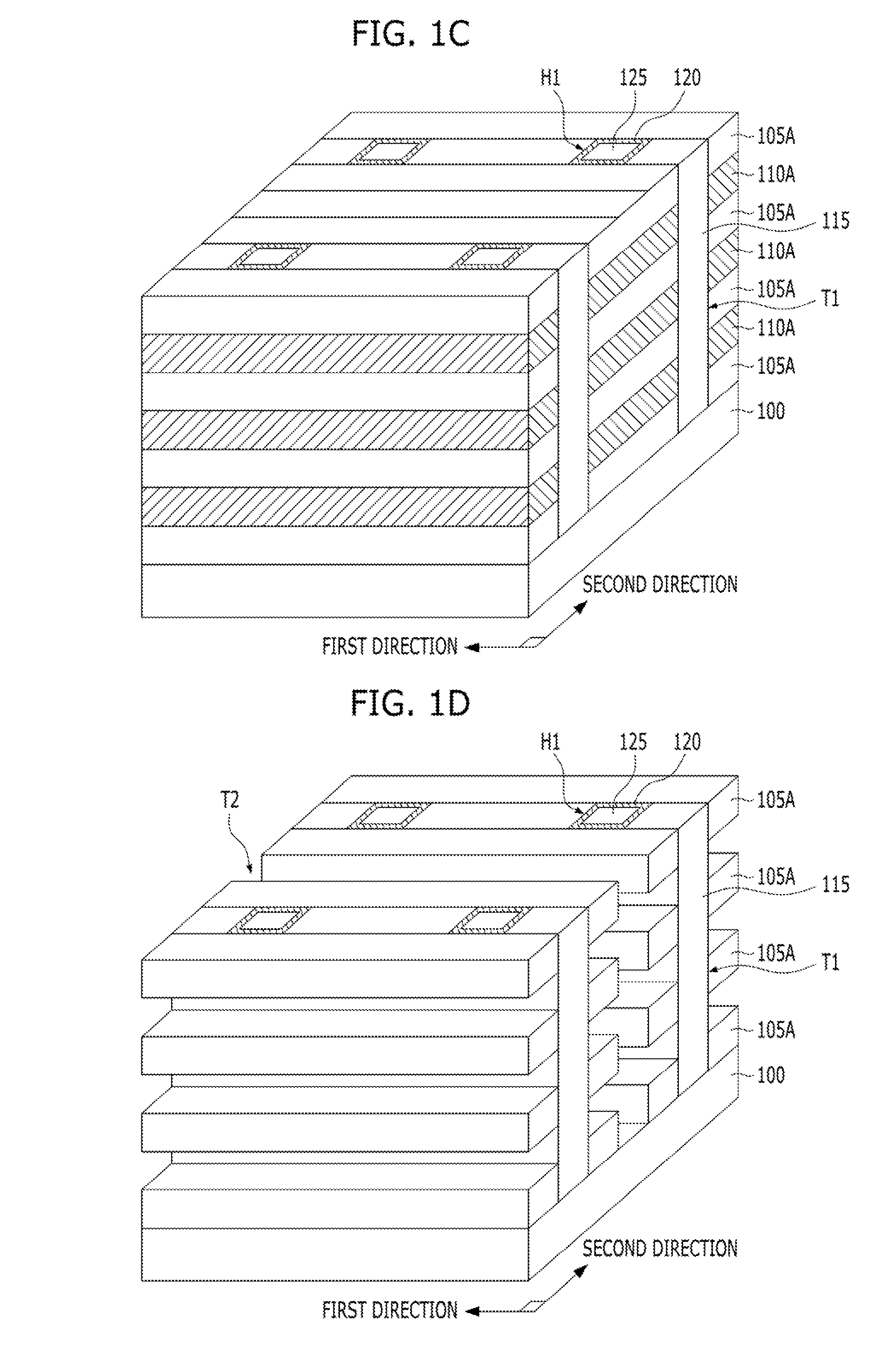
[0072]FIGS. 3A and 3B are perspective views explaining a variable resistance memory device and a method for fabricating the same in accordance with a third embodiment of the present invention. In describing the third embodiment, detailed descriptions for substantially the same component parts as the aforementioned first and second embodiments will be omitted. First, after performing the processes of FIGS. 1A and 1B of the first embodiment or the processes of FIGS. 2A and 2B of the second embodiment, the process of FIG. 3A is performed.
[0073]Referring to FIG. 3A, by selectively etching the first dielectric layer 115, first holes H1 are defined to expose the side surfaces of the first interlayer dielectric layer patterns 105A and the substrate 100....
PUM
| Property | Measurement | Unit |
|---|---|---|
| variable resistance | aaaaa | aaaaa |
| resistance | aaaaa | aaaaa |
| electrical resistance | aaaaa | aaaaa |
Abstract
Description
Claims
Application Information
 - Generate Ideas
- Intellectual Property
- Life Sciences
- Materials
- Tech Scout
- Unparalleled Data Quality
- Higher Quality Content
- 60% Fewer Hallucinations
Browse by: Latest US Patents, China's latest patents, Technical Efficacy Thesaurus, Application Domain, Technology Topic, Popular Technical Reports.
© 2025 PatSnap. All rights reserved.Legal|Privacy policy|Modern Slavery Act Transparency Statement|Sitemap|About US| Contact US: help@patsnap.com


