
Power supply circuit and semiconductor device including the same

Active Publication Date: 2013-10-31
SEMICON ENERGY LAB CO LTD
View PDF2 Cites 16 Cited by
  • Summary
  • Abstract
  • Description
  • Claims
  • Application Information

AI Technical Summary

Benefits of technology

The present invention is aimed at providing a power supply circuit that can reduce power consumption. It achieves this by using an electric storage device that can temporarily store power from the voltage regulator, which in turn reduces the supply of power to the control circuit. This prevents power consumption from charging and discharging of the voltage regulator's capacitance. The invention also includes a switch that can be turned on or off to determine its operating state, which is maintained using a transistor with extremely low off-state current. As a result, the power consumption of the power supply circuit is reduced while the control circuit is in operation. The invention can be implemented in a semiconductor device, leading to low power consumption.

Problems solved by technology

Thus, even when the switch is off, that is, even when voltage is not supplied to the load, the circuit regulating voltage is always in an operating state only to supply voltage to the control circuit, so that power is consumed.
Thus, in the circuit regulating voltage, the capacitance of the semiconductor element, a wiring, or the like is inevitably increased, so that power consumed by charging and discharging of the capacitance at the time of operating the circuit regulating voltage becomes too high to ignore.

Method used


Image

  • Power supply circuit and semiconductor device including the same
  • Power supply circuit and semiconductor device including the same
  • Power supply circuit and semiconductor device including the same

Examples


embodiment 1

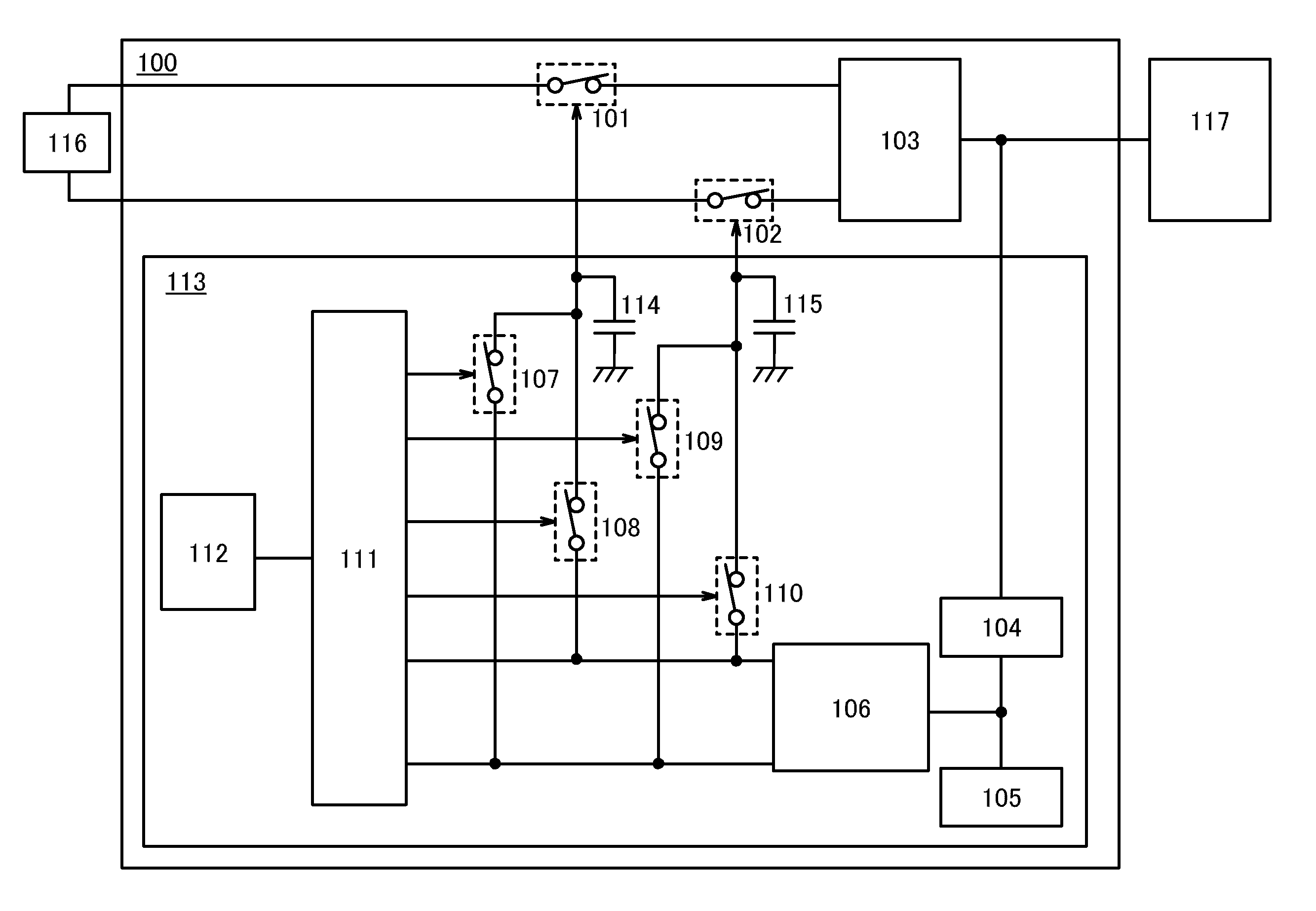
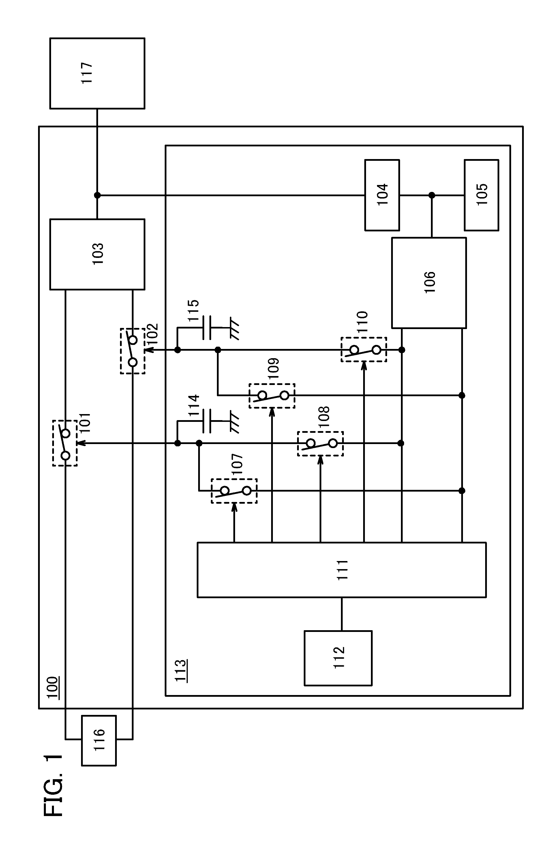
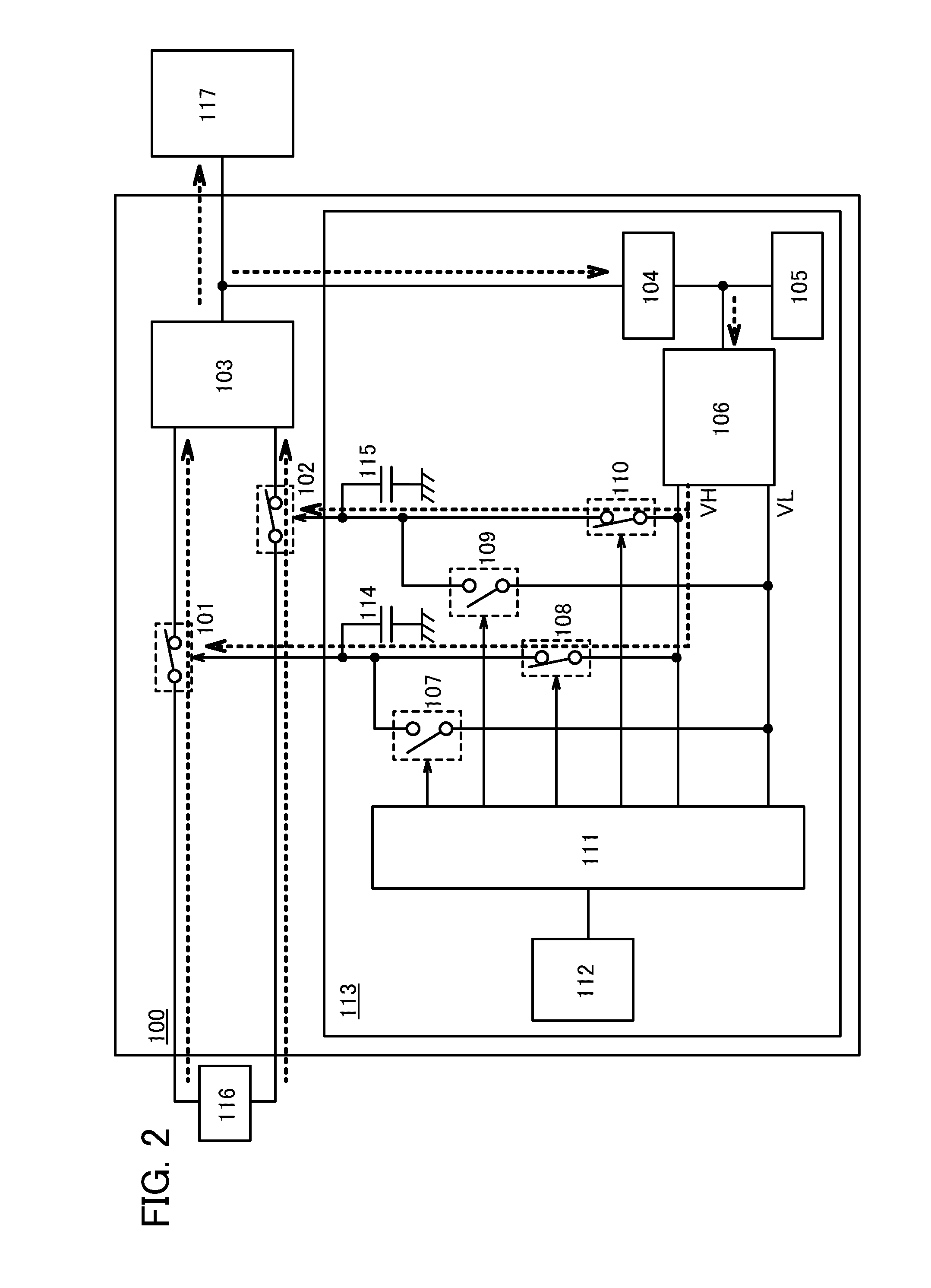
[0034]FIG. 1 illustrates a structure example of a power supply circuit 100 according to one embodiment of the present invention. The power supply circuit 100 in FIG. 1 includes a power switch 101, a power switch 102, a voltage regulator 103, and a control circuit 113.

[0035]Voltage is supplied from a power supply 116 to the power supply circuit 100. The power switches 101 and 102 each have a function of controlling input of the voltage to the voltage regulator 103. Specifically, the voltage corresponds to a difference between a first potential input from the power supply 116 to the voltage regulator 103 through the power switch 101 and a second potential input from the power supply 116 to the voltage regulator 103 through the power switch 102.

[0036]Note that in the case where the voltage output from the power supply 116 is AC voltage, as illustrated in FIG. 1, the power switch 101 controlling input of the first potential to the voltage regulator 103 and the power switch 102 controlli...

embodiment 2

[0084]In this embodiment, a more specific structure example of the power supply circuit 100 in FIG. 1 is described.

[0085]FIG. 6 illustrates a structure example of the power supply circuit 100 according to one embodiment of the present invention. The power supply circuit 100 in FIG. 6 includes a transistor 101a functioning as the power switch 101, a transistor 102a functioning as the power switch 102, the voltage regulator 103, and the control circuit 113.

[0086]Note that in FIG. 6, one transistor 101a and one transistor 102a are used as the power switch 101 and the power switch 102, respectively; however, in the power supply circuit 100 according to one embodiment of the present invention, a plurality of transistors may be used as the power switch. For example, the use of a plurality of transistors connected in parallel can achieve a power switch capable of controlling higher power.

[0087]In this specification, a state where transistors are connected to each other in parallel means a ...

embodiment 3

[0139]FIG. 9 illustrates an example of part of a cross-sectional structure of a power supply circuit according to one embodiment of the present invention. Note that FIG. 9 illustrates the transistor 107a and the capacitor 114 in FIG. 6 and the transistor 140 and the resistor 142 in FIG. 8.

[0140]In this embodiment, the transistor 140 and the resistor 142 are formed in a single crystal silicon substrate, and the transistor 107a including an oxide semiconductor in an active layer and the capacitor 114 are formed above the transistor 140 and the resistor 142. The transistor 140 may include a thin semiconductor film of silicon, germanium, or the like in an amorphous, microcrystalline, polycrystalline, or signal crystal state for an active layer. Alternatively, the transistor 140 may include an oxide semiconductor in the active layer. In the case where the transistors each include an oxide semiconductor in an active layer, the transistor 107a is not necessarily stacked above the transisto...


PUM

PropertyMeasurementUnit
Band gapaaaaaaaaaa
Electric potential / voltageaaaaaaaaaa

Abstract

A power supply circuit includes a first switch, a voltage regulator circuit connected to the first switch, and a control circuit for controlling the first switch. The control circuit includes a second switch, a third switch, and a voltage generation circuit. For controlling the first switch, first voltage output from the voltage generation circuit is applied to the first switch through the second switch, and second voltage output from the voltage generation circuit is applied to the first switch through the third switch. Power consumption of the power supply circuit can be reduced.

Description

BACKGROUND OF THE INVENTION[0001]1. Field of the Invention[0002]The present invention relates to power supply circuits including transistors as switches and semiconductor devices including the power supply circuits.[0003]2. Description of the Related Art[0004]A power supply circuit (also referred to as a power conversion circuit) has a function of regulating voltage supplied from a battery or a power supply such as a commercial power supply in accordance with the specification of a load. For example, voltage supplied from a commercial power supply is AC voltage having an effective value of 100 Vrms. In contrast, voltage needed in a commonly-used electronic device is a comparatively low DC voltage of 5 V, 12 V, or the like in many cases. In that case, voltage output from a power supply is rectified and stepped down by a power supply circuit and then supplied to a load.[0005]In general, a power supply circuit includes a circuit regulating voltage, such as a rectifier circuit, a smooth...

Claims


Application Information

Patent Timeline
IPC IPC(8): H03K17/56H02M1/00
CPCH03K17/56H02M7/217H03K17/063H03K19/0013H02M1/0006
Inventor KOYAMA, JUNSAKATA, JUNICHIRO
Owner SEMICON ENERGY LAB CO LTD
Learn More