
Method and apparatus for performing heterodyne lock-in imaging and quantitative non-contact measurements of electrical properties

a heterodyne lock-in and electrical property technology, applied in the field of optical characterization of solar cells, can solve the problems of not meeting the needs of mass production, dc pl cannot monitor the optoelectronic carrier kinetics of surface and near-subsurface regions, and is much more time-consuming

Active Publication Date: 2013-10-24
MANDELIS ANDREAS +1
View PDF1 Cites 33 Cited by
  • Summary
  • Abstract
  • Description
  • Claims
  • Application Information

AI Technical Summary

Benefits of technology

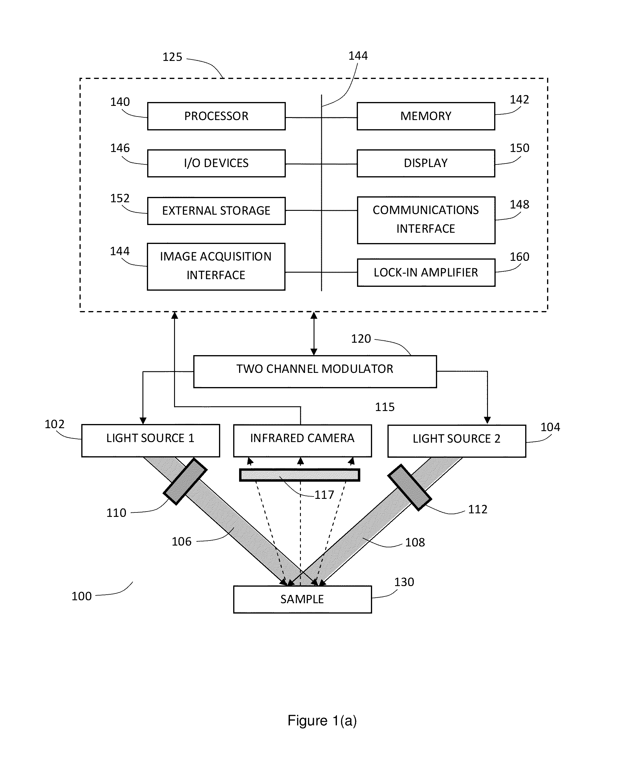
The patent text describes methods for producing optical carrierographic images of a semiconductor sample and measuring the effective lifetime of carriers in a solar cell using lock-in-carrierography. The methods involve using focused and spatially overlapped optical beams to excite carriers across the sample, and detecting the infrared radiation emitted from the sample. The detected signals are processed with a lock-in amplifier to obtain an amplitude and phase signal, which can be used to create carrierographic images of the sample. The methods provide a non-destructive and non-contact way to measure the properties of semiconductor samples.

Problems solved by technology

This practice cannot meet the needs of mass production.
Microwave photoconductance decay (MW-PCD) is a “golden standard” method for imaging lifetimes, including short recombination lifetimes, but it is much more time-consuming [17].
However, DC PL cannot monitor the optoelectronic carrier kinetics of surface and near-subsurface regions due to its depth-integrated character through the signal dependence on the DC carrier diffusion length [3].

Method used


Image

  • Method and apparatus for performing heterodyne lock-in imaging and quantitative non-contact measurements of electrical properties
  • Method and apparatus for performing heterodyne lock-in imaging and quantitative non-contact measurements of electrical properties
  • Method and apparatus for performing heterodyne lock-in imaging and quantitative non-contact measurements of electrical properties

Examples


example 1

DC Photoluminescence, Direct and Heterodyne Lock-in Carrierography of a Multicrystalline Solar Cell and a Silicon Wafer

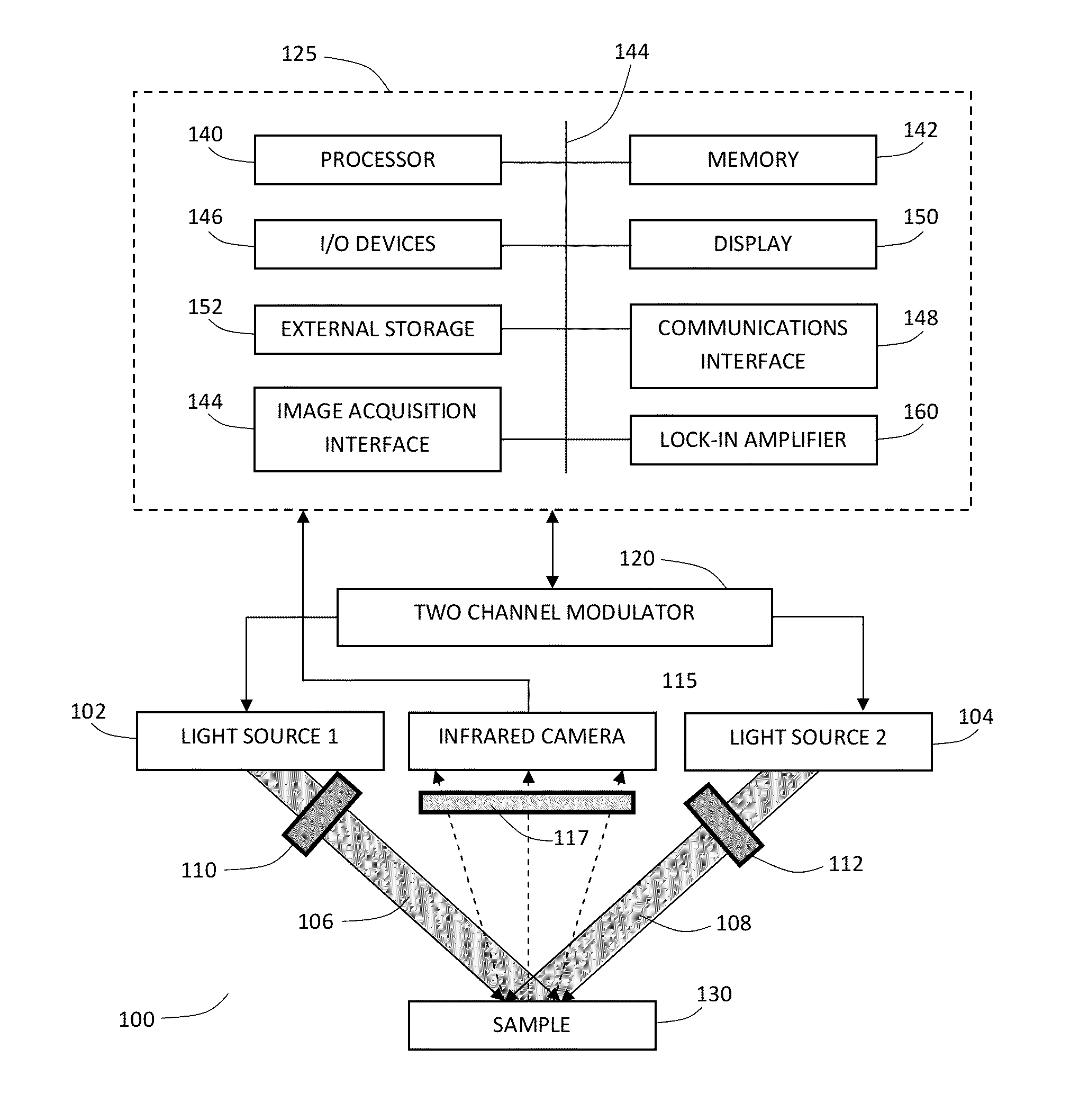
[0189]To highlight the features of lock-in HDC, compared to conventional optoelectronic imaging methods such as DC photoluminescence and direct LIC, experimental results with these imaging methods and heterodyne lock-in carrierography of multicrystalline Si solar cell of various dimensions are shown in FIGS. 7-10.

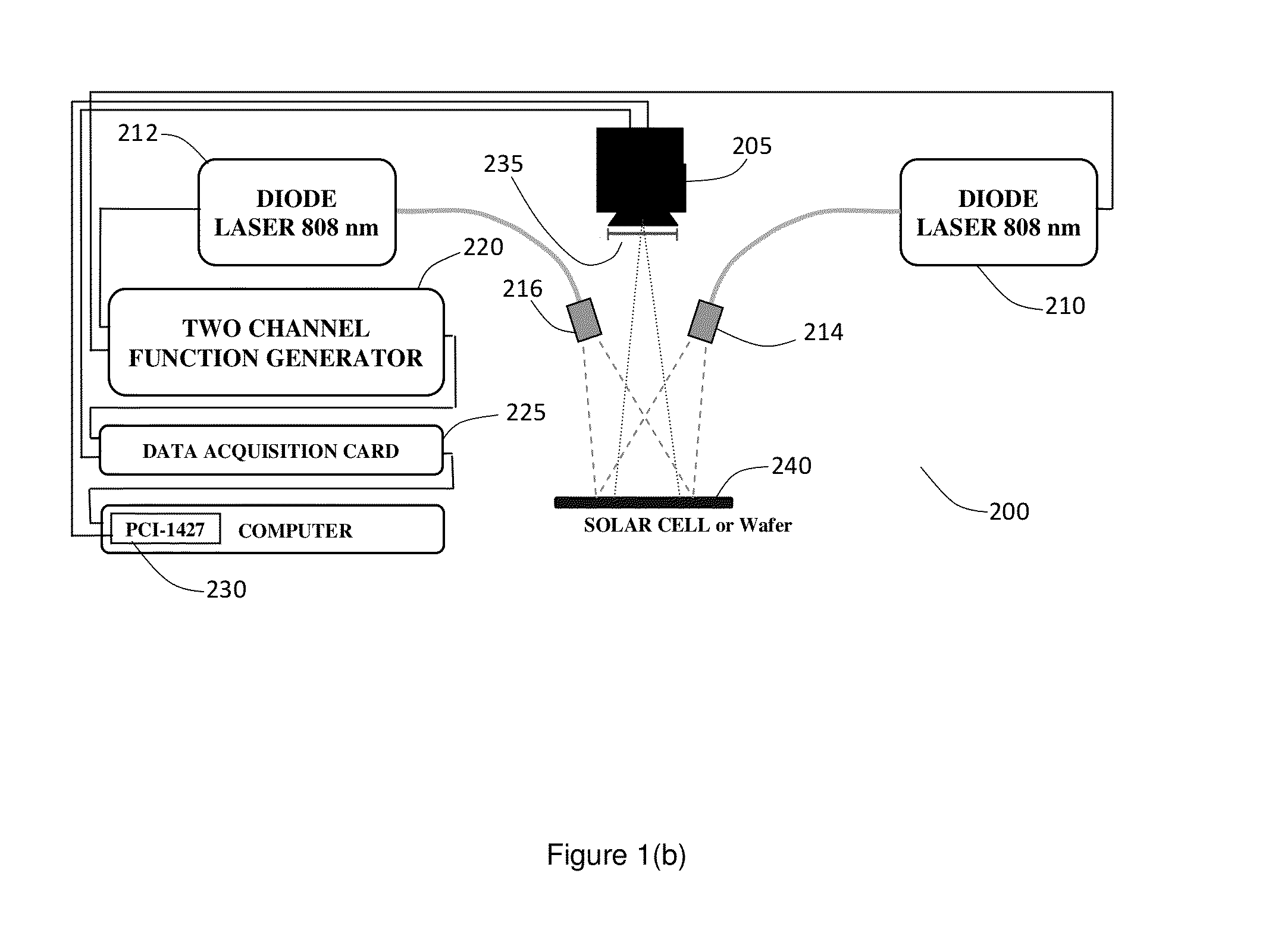
[0190]The apparatus 200 employed to perform the carrierographic measurements is shown in FIG. 1(b), and consisted of a high-speed NIR InGaAs snapshot camera 205 with windowing, two fiber coupled 808-nm 9-W diode lasers 210 and 212, optical blocks 214 and 216 with collimator and diffuser, a two-channel function generator 220, a data acquisition module 225 and a frame grabber 230. A long-pass filter 235 is used to prevent the excitation laser beams from interfering with the NIR camera 200.

[0191]The near infrared InGaAs camera employed (SU320KTSW-1.7RT / RS170 f...

example 2

Statistical Optoelectronic Quality Monitoring Method Via Lock-in Heterodyne Carrierography Imaging

[0204]Statistical distributions of direct and heterodyne lock-in amplitudes of two mc Si solar cells can be generated and are shown in FIG. 12. The statistical distribution was created by counting the number of pixels with amplitude within the range a and a+(bin size), that is proportional to the area of a solar cell or a substrate with pixel amplitudes within this range. The statistical distribution of the direct lock-in carrierography amplitude clearly shows the fraction of the area which does not generate photocurrent. This method of surface-integrated carrierographic amplitude (Sum of pixels) characterizes the optoelectronic quality of a solar cell. The statistical distribution heterodyne lock-in carrierography amplitude shows similar trends. However, the heterodyne carrierography images provide more features compared with the direct lock-in images as will be shown below.

example 3

Correlation Between Heterodyne Lock-in Image and Lifetime Map of MC Silicon Solar Cell

[0205]It follows from the foregoing theory (Eqs. 9, 11, 23, 24, 29, 30) that the heterodyne signal depends on the transport parameters of a solar cell as well as the nonlinearity coefficient γ. The most important transport parameter is the bulk recombination lifetime. For experimental confirmation of this correlation, the same fragment of a solar cell was measured with the help of a conventional technique: A map of recombination lifetimes was generated using the microwave reflectance PCD (μ-PCD) technique with a Semilab WT2000 system and is shown in FIG. 15.

[0206]The 10-Hz direct lock-in and heterodyne lock-in carrierographic images of the same area are shown in FIG. 16 and FIG. 17, respectively.

[0207]It is seen that lower-frequency carrierographic amplitude images correlate with the lifetime map. Areas with higher amplitude correspond to areas with higher recombination lifetime. The HDC images sho...


PUM


Abstract

Methods are provided for producing optical carrierographic images of a semiconductor sample. Focused and spatially overlapped optical beams excite carriers across within the semiconductor sample, where the optical beams are modulated such that a beat frequency is substantially less than either modulation frequency. An infrared detector detects infrared radiation emitted from the semiconductor sample in response to absorption of the optical beams, thereby obtaining a plurality of carrierographic signals at different points in time during at least one beat period, which are processed with a lock-in amplifier, with a reference signal at the beat frequency, to obtain an amplitude signal and a phase signal. Carrierographic lock-in images of the sample are obtained in a scanning configuration, or in an imaging format using an imaging detector. The images carry quantitative information about recombination lifetimes in substrate Si wafers and electrical parameters in solar cells, namely photogeneration current density, diode saturation current density, ideality factor, and maximum power photovoltage.

Description

CROSS-REFERENCE TO RELATED APPLICATION[0001]This application claims priority to U.S. Provisional Application No. 61 / 623,676, titled “METHOD AND APPARATUS FOR PERFORMING HETERODYNE LOCK-IN CARRIEROGRAPHIC IMAGING” and filed on Apr. 13, 2012, the entire contents of which is incorporated herein by reference.BACKGROUND[0002]The present disclosure relates apparatus and methods of non-contact, optical, characterization of semiconductors and semiconductor devices. More particularly, the present disclosure relates to the optical characterization of solar cells. The modern solar cell industry has moved toward GW-scale production, with quality control becoming a critical factor [15]. Conventionally, the I-V characteristics are obtained by attaching a resistive load or a power source to the irradiated solar cell to measure and evaluate its efficiency. This practice cannot meet the needs of mass production.[0003]Non-destructive and non-contacting methods for optoelectronic diagnostics of solar ...

Claims


Application Information

Patent Timeline
Patent Type & Authority Applications(United States)
IPC IPC(8): H04N5/33
CPCH04N5/33G01N21/6489G01N21/9501H04N23/21
Inventor MANDELIS, ANDREASMELNIKOV
Owner MANDELIS ANDREAS
Learn More