
Touch panel and method of manufacturing the same

a technology of touch panel and manufacturing method, which is applied in the direction of resistive material coating, packaging, metallic material coating process, etc., can solve the problems of difficult to reduce the separation distance of the touch panel, the crossing area of the driving channel, and the difficulty of reducing the crossing distance of the sensing channel, so as to reduce the thickness of the touch panel without deterioration of the touch performance, the effect of simplifying the production process

Inactive Publication Date: 2013-10-24
SAMSUNG ELECTRONICS CO LTD
View PDF14 Cites 18 Cited by
  • Summary
  • Abstract
  • Description
  • Claims
  • Application Information

AI Technical Summary

Benefits of technology

The present invention provides a touch panel and a method of manufacturing the same that addresses problems associated with thick and unflexible touch panels. The invention uses a conductive mesh to create a driving channel and sensing channel, reducing the thickness of the touch panel without compromising touch performance. The invention also has a lower resistance than traditional transparent electrodes, improving touch performance and allowing for larger touch panels to be produced. Additionally, the invention simplifies production processes and reduces production costs.

Problems solved by technology

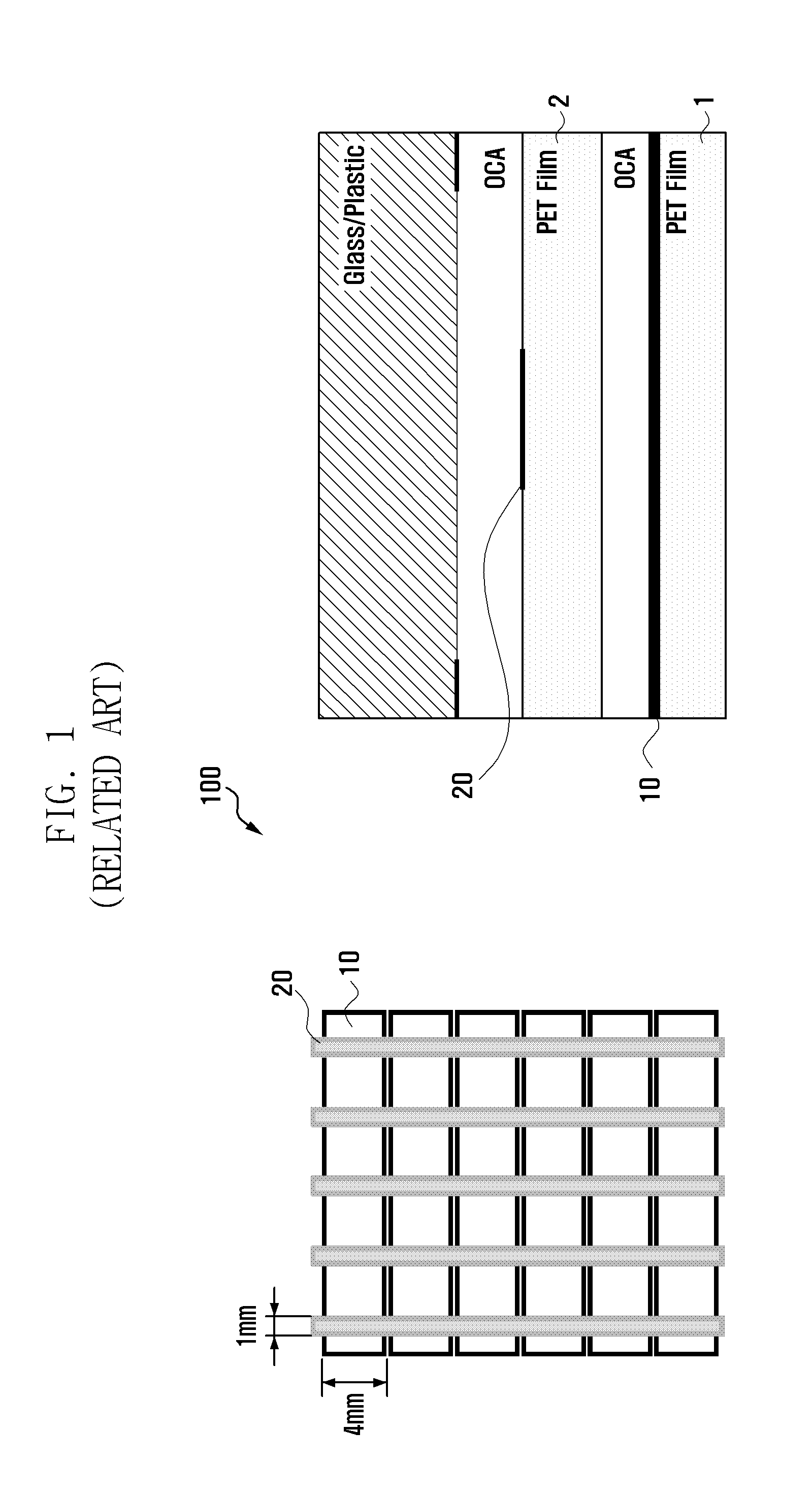
However, when using ITO, a technical limitation exists in reducing a crossing area of the driving channel 10 and the sensing channel 20.
Particularly, when using a substrate having a large dielectric constant, it is difficult to reduce a separation distance in the touch panel 100.

Method used


Image

  • Touch panel and method of manufacturing the same
  • Touch panel and method of manufacturing the same
  • Touch panel and method of manufacturing the same

Examples


Embodiment Construction

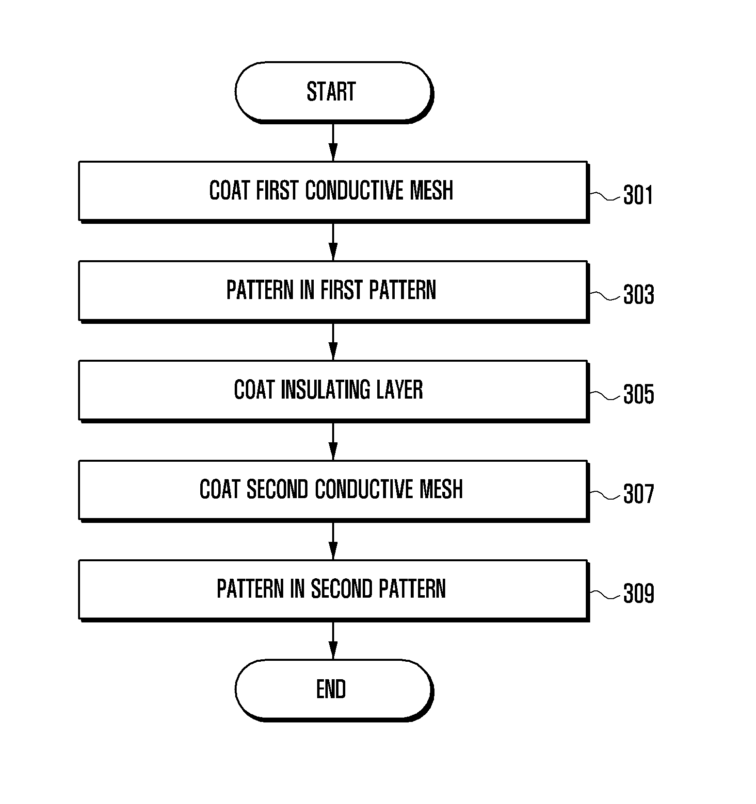
[0038]The following description with reference to the accompanying drawings is provided to assist in a comprehensive understanding of exemplary embodiments of the invention as defined by the claims and their equivalents. It includes various specific details to assist in that understanding but these are to be regarded as merely exemplary. Accordingly, those of ordinary skill in the art will recognize that various changes and modifications of the embodiments described herein can be made without departing from the scope and spirit of the invention. In addition, detailed descriptions of well-known functions and constructions may be omitted for clarity and conciseness.

[0039]The terms and words used in the following description and claims are not limited to the bibliographical meanings, but, are merely used by the inventor to enable a clear and consistent understanding of the invention. Accordingly, it should be apparent to those skilled in the art that the following description of exempl...


PUM

PropertyMeasurementUnit
Flexibilityaaaaaaaaaa
Electrical conductoraaaaaaaaaa
Widthaaaaaaaaaa

Abstract

A touch panel using a conductive mesh and a method of manufacturing the same are provided. The touch panel includes a substrate on which a conductive mesh is disposed, a plurality of driving channels for recognizing a horizontal axis coordinate, wherein the plurality of driving channels are formed by patterning a first conductive mesh disposed on the substrate, a plurality of sensing channels for recognizing a vertical axis coordinate, wherein the sensing channels are formed by patterning a second conductive mesh disposed on the substrate, and an insulating layer positioned between the first conductive mesh and the second conductive mesh.

Description

PRIORITY[0001]This application claims the benefit under 35 U.S.C. §119(a) of a Korean patent application filed on Apr. 23, 2012 in the Korean Intellectual Property Office and assigned Serial No. 10-2012-0041883, the entire disclosure of which is hereby incorporated by reference.BACKGROUND OF THE INVENTION[0002]1. Field of the Invention[0003]The present invention relates to a touch panel and a method of manufacturing the same. More particularly, the present invention relates to a touch panel using a conductive mesh and a method of manufacturing the same.[0004]2. Description of the Related Art[0005]Nowadays, due to convenience to input data into an apparatus, interest has increased in a touch screen. The touch screen is formed by attaching a touch panel at a front surface of a display panel. That is, the touch screen can perform an input function and a display function. Particularly, nowadays, interest has increased in a multi-touch panel that can simultaneously recognize a plurality ...

Claims


Application Information

Patent Timeline
IPC IPC(8): G06F3/041
CPCG06F3/0412G06F2203/04103Y10T156/10G06F3/0445G02F1/13338G06F2203/04111G06F3/0446G06F3/0416H10K59/40
Inventor KIM, HAKYEOL
Owner SAMSUNG ELECTRONICS CO LTD
Learn More