Electrode structure of capacitive touch panel
a capacitive touch panel and electrode structure technology, applied in the direction of printed circuits, printed circuit details, instruments, etc., can solve the problem of more noise sensed, and achieve the effect of increasing input signals, enhancing signal-to-noise ratio, and decreasing the noise of sensing signals
- Summary
- Abstract
- Description
- Claims
- Application Information
AI Technical Summary
Benefits of technology
Problems solved by technology
Method used
Image
Examples
first embodiment
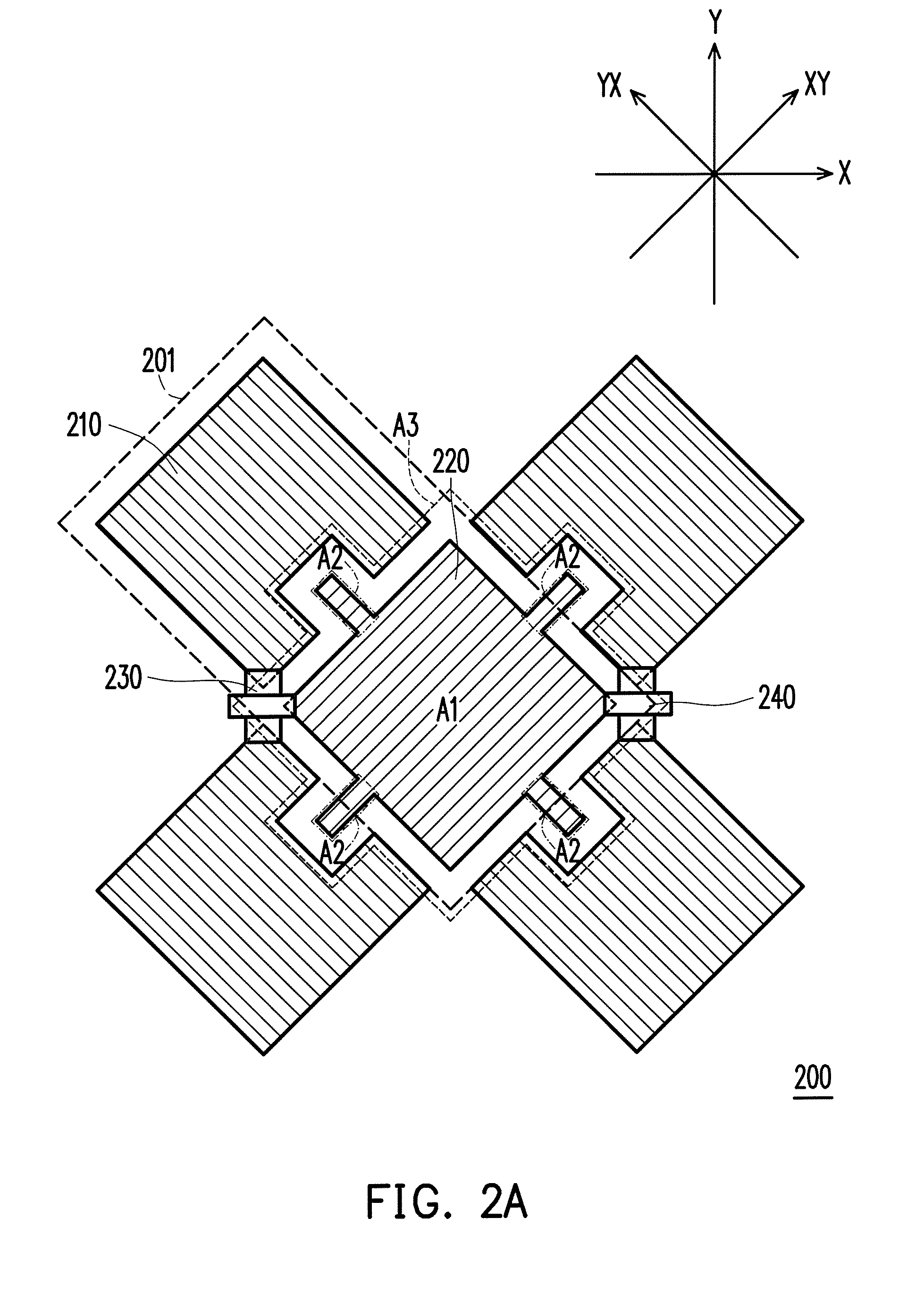
[0044]FIG. 2A is a schematic diagram of an electrode structure of a capacitive touch panel according to an embodiment of the invention, FIG. 2B and FIG. 2C are enlarged views of a part region of the electrode structure of FIG. 2A. Referring to FIG. 2A to FIG. 2C, the electrode pattern 200 of the touch panel of the present embodiment includes a plurality of receiving electrodes 210, a plurality of driving electrodes 220, a plurality of vertical electric bridges 230 and a plurality of horizontal electric bridges 240. The vertical electric bridges 230 are used to electrically connect the receiving electrodes 210 of a same column. The horizontal electric bridges 240 are used to electrically connect the driving electrodes 220 of a same row. In the present embodiment, the receiving electrodes 210 are isolated to the driving electrodes 220, and an area of each of the driving electrodes 220 is greater than an area of each of the receiving electrodes 210. Each of the receiving electrodes 210...
second embodiment
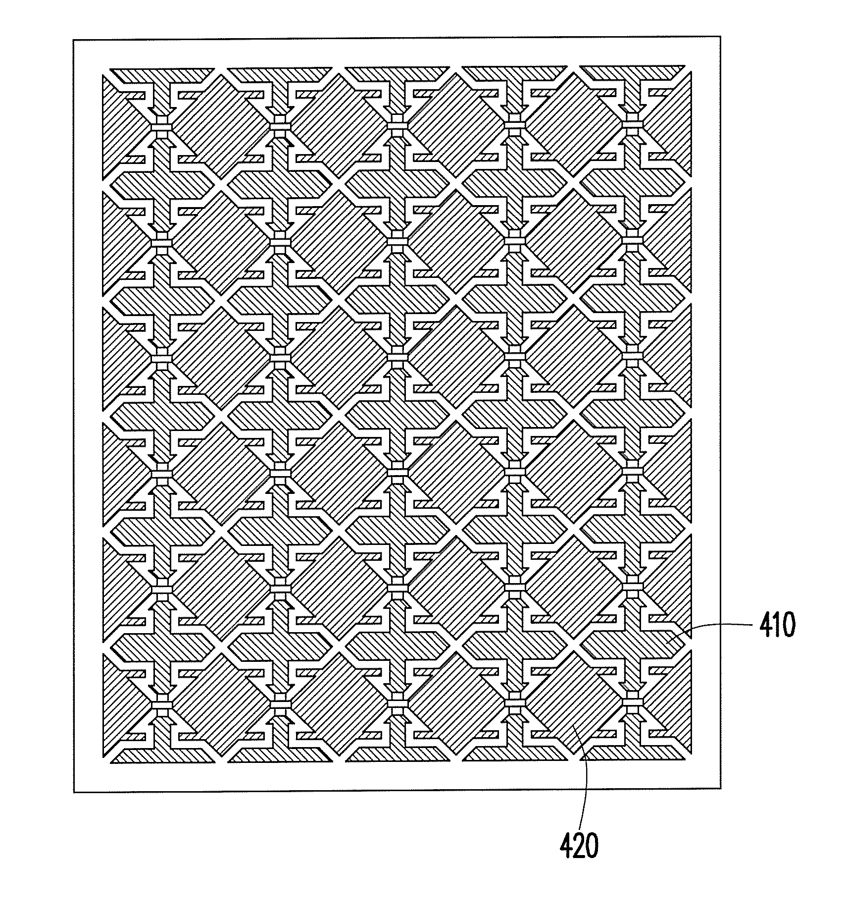
[0060]FIG. 4A is a schematic diagram of an electrode structure of a capacitive touch panel according to an embodiment of the invention, FIG. 4B and FIG. 4C are enlarged views of a part region of the electrode structure of FIG. 4A. Referring to FIG. 2A and FIG. 4A to FIG. 4C, the electrode pattern 400 of the touch panel of the present embodiment is similar to the electrode pattern 200 of the first embodiment, though a main difference there between lies in the opening directions of the openings of the receiving electrodes 410 and the elongation direction of the elongation regions A2 of the driving electrode 420. The main region A1 of the driving electrode 420 and the electrode structure of the receiving electrode 410 are as that of the main region A1 of the driving electrode 220 and the receiving electrode 210 of the first embodiment, so that details thereof are not repeated.
[0061]In detail, sizes of the four elongation regions A2 of the driving electrode 420 of the present embodiment...
third embodiment
[0066]FIG. 6A is schematic diagram of an electrode structure of a capacitive touch panel according to an embodiment of the invention, FIG. 6B and FIG. 6C are enlarged views of a part region of the electrode structure of FIG. 6A. Referring to FIG. 2A and FIG. 6A to FIG. 6C, the electrode pattern 600 of the touch panel of the present embodiment is similar to the electrode pattern 200 of the first embodiment, though a main difference there between lies in the opening directions of the openings of the receiving electrodes 610 and the elongation direction of the elongation regions A2 of the driving electrode 620. The main region A1 of the driving electrode 620 and the electrode structure of the receiving electrode 610 are as that of the main region A1 of the driving electrode 220 and the receiving electrode 210 of the first embodiment, so that details thereof are not repeated.
[0067]In detail, sizes of the four elongation regions A2 of the driving electrode 620 of the present embodiment a...
PUM
 Abstract
Description
Claims
Application Information
 - R&D
- Intellectual Property
- Life Sciences
- Materials
- Tech Scout
- Unparalleled Data Quality
- Higher Quality Content
- 60% Fewer Hallucinations
Browse by: Latest US Patents, China's latest patents, Technical Efficacy Thesaurus, Application Domain, Technology Topic, Popular Technical Reports.
© 2025 PatSnap. All rights reserved.Legal|Privacy policy|Modern Slavery Act Transparency Statement|Sitemap|About US| Contact US: help@patsnap.com


